Semiconductor device and electric power converter

a technology of semiconductor devices and electric power converters, which is applied in the direction of semiconductor devices, solid-state devices, basic electric elements, etc., can solve the problems of air bubble generation in semiconductor devices, degraded insulation performance of semiconductor devices, etc., and achieve the effect of suppressing the generation of air bubbles

Active Publication Date: 2019-07-04
MITSUBISHI ELECTRIC CORP
View PDF2 Cites 3 Cited by
  • Summary
  • Abstract
  • Description
  • Claims
  • Application Information

AI Technical Summary

Benefits of technology

[0013]According to one embodiment of the present invention, in the semiconductor device having a narrow gap, generation of air bubbles can be suppressed, and thus insulation reliability can be improved.

Problems solved by technology

In a portion in which such air bubbles are generated, the insulation filling effect by the silicone gel cannot be obtained, and hence the insulation performance of the semiconductor device is degraded.
Even when degassing processing is performed when the silicone gel is injected, there is a risk that air bubbles may be generated in the semiconductor device.

Method used


Image

  • Semiconductor device and electric power converter
  • Semiconductor device and electric power converter
  • Semiconductor device and electric power converter

Examples


first embodiment

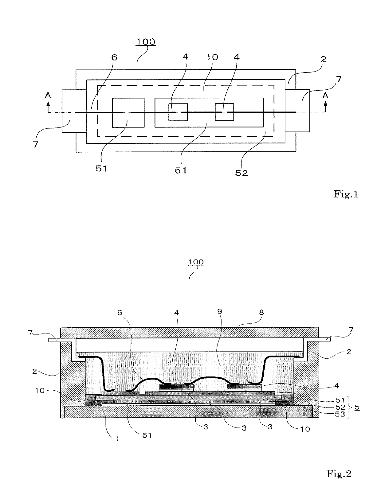
[0028]FIG. 1 is a schematic top structure view for illustrating a semiconductor device according to a first embodiment of the present invention. FIG. 2 is a schematic sectional structure view for illustrating the semiconductor device according to the first embodiment of the present invention. FIG. 1 is a view for illustrating a semiconductor device 100 as viewed from the top through a first filler 9 being a silicone composition. A peripheral edge portion (outer peripheral portion) of an insulating substrate 52, which is covered with a second filler 10, is indicated by the dotted line.

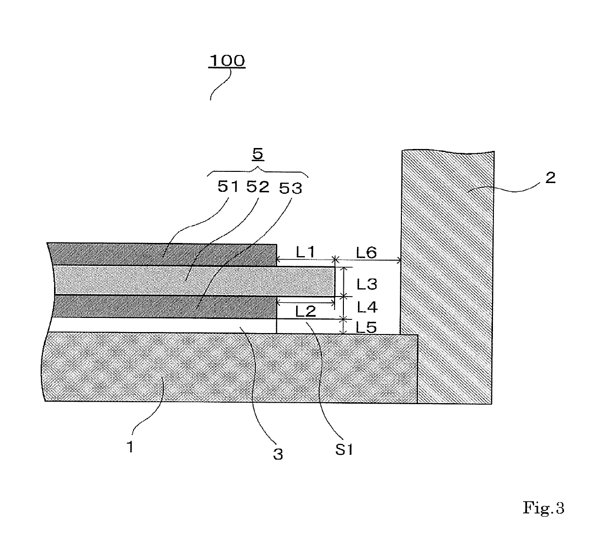
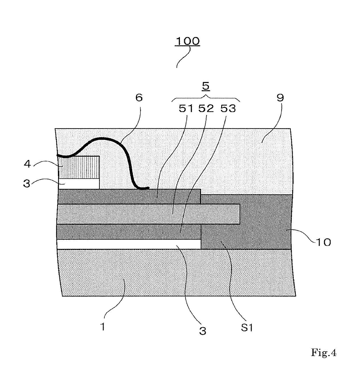
[0029]FIG. 2 is a schematic sectional structure view taken along the dash-dotted line A-A of FIG. 1. In FIG. 2, the semiconductor device 100 includes a base plate 1, a case member 2, solder 3 serving as a bonding material, semiconductor elements 4, an insulating circuit board 5, bonding wires 6 serving as wiring members, electrode terminals 7, a lid member 8, the first filler 9 being a silicone composit...

second embodiment

[0071]A second embodiment of the present invention differs from the first embodiment in that a plurality of insulating circuit boards 5 used in the first embodiment are arranged in the case. Other points are similar to those in the first embodiment, and hence detailed description thereof is omitted. Even when a plurality of insulating circuit boards are arranged in the case as described above, the peripheral edge portions of the insulating circuit boards are filled with silicone rubber, and hence the insulation reliability of the semiconductor device can be improved.

[0072]FIG. 5 is a schematic top structure view for illustrating a semiconductor device according to a second embodiment of the present invention. FIG. 6 is a schematic sectional structure view for illustrating the semiconductor device according to the second embodiment of the present invention. FIG. 5 is a view for illustrating a semiconductor device 200 as viewed from the top through the first filler 9 being a silicone ...

third embodiment

[0088]A third embodiment of the present invention differs from of the first embodiment in that the periphery of the insulating circuit board 5 used in the first and second embodiments is surrounded by a partition wall. Other points are similar to those of the first embodiment, and hence detailed description thereof is omitted. Through surrounding of the periphery of the insulating circuit board by the partition wall as described above, the insulation reliability is affected, and a region in which filling of silicone rubber is required is filled with the silicone rubber. Therefore, the insulation reliability of the semiconductor device can be improved.

[0089]FIG. 8 is a schematic top structure view for illustrating a semiconductor device according to the third embodiment of the present invention. FIG. 9 is a schematic sectional structure view for illustrating the semiconductor device according to the third embodiment of the present invention. FIG. 8 and FIG. 9 are illustrations of a c...


PUM


Abstract

A semiconductor device including: an insulating substrate having a conductor layer on the upper face and the lower face and a semiconductor element mounted on the upper conductor layer; a base plate bonded to the lower conductor layer; a case member surrounding the insulating substrate and bonded to the surface of the base plate to which the conductor layer bonded to the lower face; a first filler being a silicone composition filled in a region surrounded by the base plate and the case member; and a second filler being injected into a region below the first filler and surrounding a peripheral edge portion of the insulating substrate, whose height from the base plate is higher than the upper face and is lower than a bonding face between the semiconductor element and the upper conductor layer.

Description

TECHNICAL FIELD[0001]The present invention relates to a filling structure of a semiconductor device in which a power semiconductor element is sealed with a filler, and to an electric power converter using the semiconductor device.BACKGROUND ART[0002]A semiconductor element of a type in which an energization path is formed in a vertical direction of the element for the purpose of coping with a high voltage and a large current is generally called a power semiconductor element (for example, an insulated gate bipolar transistor (IGBT), a metal oxide semiconductor field effect transistor (MOSFET), a bipolar transistor, or a diode). A semiconductor device in which the power semiconductor element is mounted on a circuit board and packaged with a filler is used in various fields, such as industrial equipment, vehicles, and railways. In recent years, along with increase in performance of equipment having the semiconductor device mounted thereon, there is more demand for increase in performan...

Claims


Application Information

Patent Timeline
Patent Type & Authority Applications(United States)
IPC IPC(8): H01L23/24H01L23/049H01L23/373H01L23/00H01L25/07H02M7/5387
CPCH01L23/24H01L23/049H01L23/3735H01L23/562H01L24/73H01L25/072H02M7/53871H01L2224/73265H01L2924/10254H01L2924/10272H01L2924/1033H01L2924/13091H01L2924/1203H01L2924/14252H01L2924/3512H01L2924/3641H02P27/08H01L2924/181H01L2224/48137H01L2224/48472H01L2924/16195H01L2924/19107H01L23/04H01L24/29H01L24/32H01L24/45H01L24/48H01L24/49H01L2224/32225H01L2224/45014H01L2224/45015H01L2224/45124H01L2224/45144H01L2224/45147H01L2224/48227H01L2224/48247H01L2224/49109H01L2224/85205H01L2224/85801H01L2224/29101H01L2924/13055H01L23/057H02M7/003H01L2924/00012H01L2924/00014H01L2924/2076H01L2924/014H01L2924/00H01L23/31H01L23/10H01L25/07H01L25/18H01L23/28H01L23/29
Inventor HARADA, HIROYUKIHARADA, KOZOSHIOTA, HIROKIYAMAGUCHI, YOSHIHIROYAMADA, KOJI
Owner MITSUBISHI ELECTRIC CORP
Why Eureka
Try Eureka