Touch OLED display panel and display device

a display panel and touch technology, applied in the field of display technology, can solve the problems of low light transmittance and thickness of the display panel, and achieve the effects of high light transmittance, thin thickness, and simple structur

Inactive Publication Date: 2019-07-25
WUHAN CHINA STAR OPTOELECTRONICS TECH CO LTD
View PDF4 Cites 1 Cited by
  • Summary
  • Abstract
  • Description
  • Claims
  • Application Information

AI Technical Summary

Benefits of technology

[0017]According to the touch type OLED display panel and the display device provided in the embodiments of the present disclosure, the touch structure is arranged in the OLED display panel. Specifically, the touch structure is arranged on a side of the package cover far away from the flexible array substrate to form an on-cell touch structure, which has the advantages of simple structure, thin thickness and high light transmittance. In addition, in the non-display area of the display panel, the flexible array substrate is bent and connected to the package cover, so that the two are electrically connected. Thereby, the same chip bonding portion can be shared by a display driver and a touch driver, which not only reduces the difficulty of the bonding process but also reduces the cost.

Problems solved by technology

This touch OLED display device has the disadvantages of low light transmittance and thick.

Method used


Image

  • Touch OLED display panel and display device
  • Touch OLED display panel and display device
  • Touch OLED display panel and display device

Examples


embodiment 1

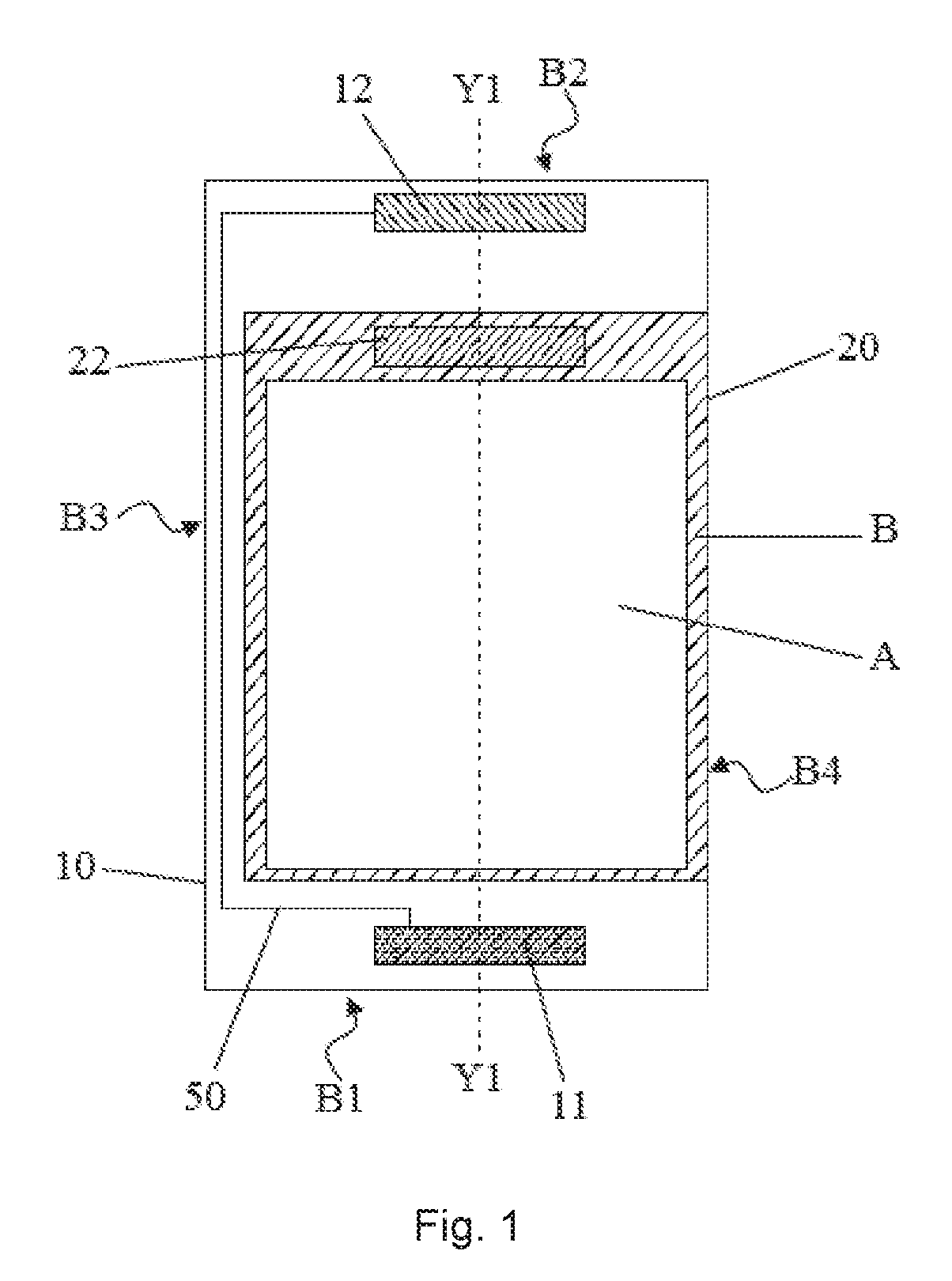
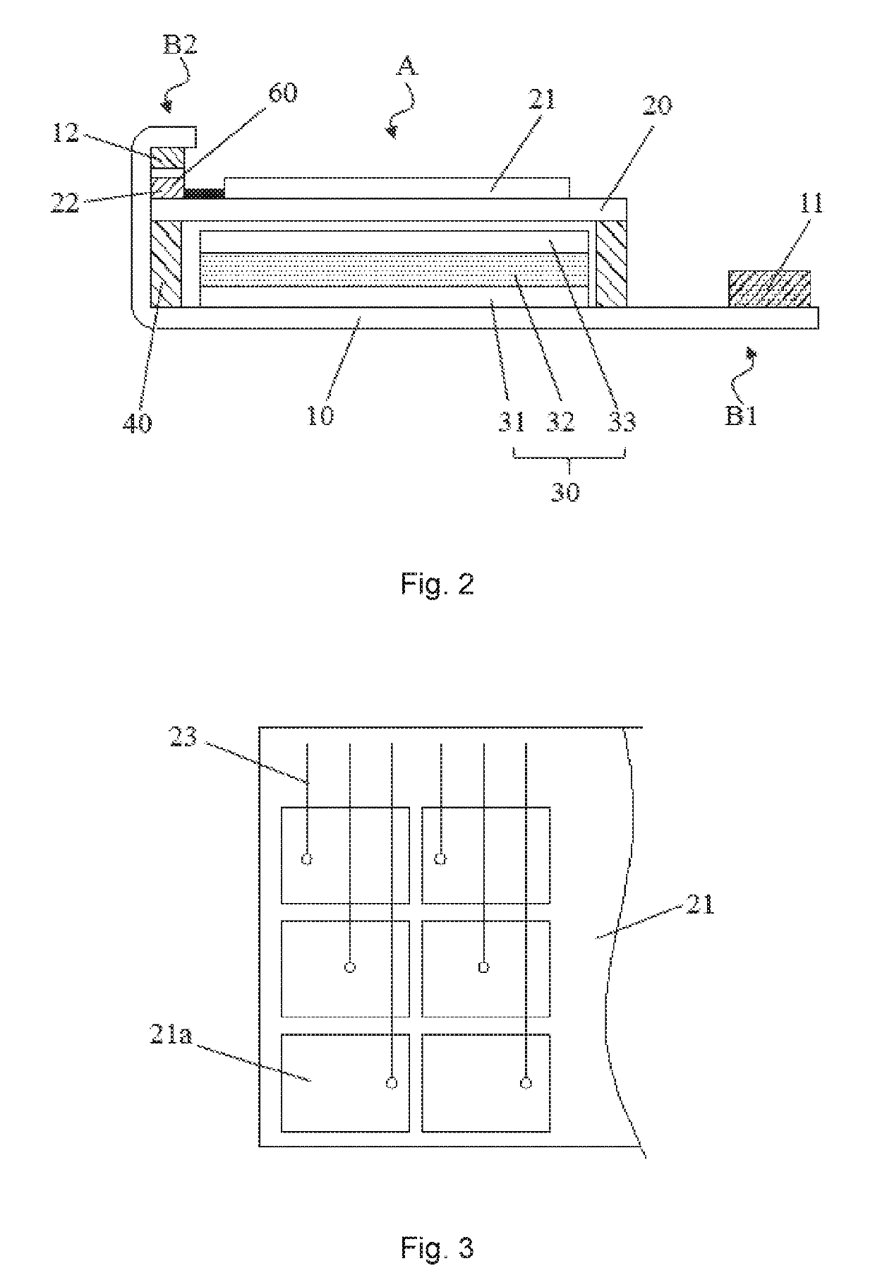
[0030]The present embodiment provides a touch OLED display panel, refer to FIG. 1 and FIG. 2, the touch OLED display panel includes a flexible array substrate 10 and a package cover 20 opposite to each other, an organic light emitting structure layer 30 and a sealant 40 arranged between the flexible array substrate 10 and the package cover 20. Wherein the sealant 40 is arranged around the organic light emitting structure layer 30, the flexible array substrate 10, the package cover 20 and the sealant 40 together form a sealed chamber, the organic light emitting structure layer 30 is arranged in the sealed chamber. The organic light emitting structure layer 30 includes an anode layer 31, a luminescent material layer 32 and a cathode layer 33 arranged on the flexible array substrate 10 sequentially.

[0031]Wherein the base substrate of the flexible array substrate 10 is a flexible substrate, for example, a flexible substrate formed of a polymer material such as Polyimide (PI), Polycarbon...

embodiment 2

[0041]The present embodiment provides a touch OLED display panel, different from Embodiment 1, referring to FIG. 5 to FIG. 7, on the flexible array substrate 10, the chip bonding portion 11 is arranged on a first side B1 outside the display area A, the first connection terminal 12 is arranged on the third side B3 adjacent the first side B1 outside the display area A. on the package cover 20, the second connection terminal 22 is arranged on the third side B3 adjacent the first side B1 outside the display area A, and opposite to the position of the first connection terminal 12. It is easy to understand that the first connection terminal 12 and the second connection terminal 22 may also be arranged on the other side adjacent the first side B1, that is the fourth side B4.

[0042]Wherein the side (third side B3) of the flexible array substrate 10 arranged with the first connection terminal 12 is bent and connected on the package cover 20, the second connection terminal 22 and the first con...

embodiment 3

[0045]The present embodiment provides a touch OLED display panel. Different from Embodiment 1 and Embodiment 2, referring to FIG. 8 and FIG. 9, on the flexible array substrate 10, the chip bonding portion 11 is arranged on the first side B1 outside the display area A, and the first connection terminal 12 is arranged on the third side B3 and the fourth side B4 outside the display area A. Correspondingly, on the package cover 20, the third side B3 and the fourth side B4 outside the display area A are also provided with the second connection terminal 22.

[0046]Wherein the side (third side B3 and fourth side B4) of the flexible array substrate 10 arranged with the first connection terminal 12 is bent and connected on the package cover 20, the second connection terminal 22 and the first connection terminal are electrically connected to each other, specifically, the first connection terminal 12 on the third side B3 is connected to the second connection terminal 22 on the third side B3, the...


PUM


Abstract

The present disclosure discloses a touch OLED display panel including a flexible array substrate, a package cover and a display area; wherein a chip bonding portion and a first connection terminal are electrically connected to each other, a touch electrode and a second connection terminal are electrically connected to each other on a side of the package cover, the chip bonding portion and the first connection terminal are respectively located at two different sides outside the display area, and the first connection terminal and the second connection terminal are located at a same side outside the display area. A side of the flexible array substrate arranged with the first connection terminal is bent and connected to the package cover, and the second connection terminal and the first connection terminal are electrically connected to each other. The present disclosure further discloses a display device including the touch OLED display panel.

Description

RELATED APPLICATIONS[0001]The present application is a National Phase of International Application Number PCT / CN2017 / 111059, filed Nov. 15, 2017, and claims the priority of China Application No. 201711057699.5, filed Nov. 1, 2017.FIELD OF THE DISCLOSURE[0002]The present disclosure relates to a display technology field, and more particularly to a touch OLED display panel and a display device.BACKGROUND OF THE DISCLOSURE[0003]With the development of the information age and the accelerating pace of life, touch technology has gradually replaced the traditional mouse and keyboard because of its user-friendly design and simple and quick input. It has been widely applied to a wide range of electronic products. Wherein the capacitive touch screen due to its advantages of fast response, high sensitivity, high reliability and durability are widely used.[0004]OLED (Organic Light Emitting Diode) display device has self-luminous, wide viewing angle, high luminous efficiency, low power consumptio...

Claims


Application Information

Patent Timeline
Patent Type & Authority Applications(United States)
IPC IPC(8): H01L27/32G06F3/041H01L51/00H01L51/52
CPCH01L27/323G06F3/0412H01L51/0097H01L51/5203G06F3/041G06F3/0443G06F3/0446Y02E10/549H10K59/40H10K2102/311G06F3/044H10K50/805H10K77/111
Inventor TANG, YUEJUN
Owner WUHAN CHINA STAR OPTOELECTRONICS TECH CO LTD
Why Eureka
Try Eureka