Electro-optical device, manufacturing method for electro-optical device, and electronic apparatus
- Summary
- Abstract
- Description
- Claims
- Application Information
AI Technical Summary
Benefits of technology
Problems solved by technology
Method used
Image
Examples
exemplary embodiment 2
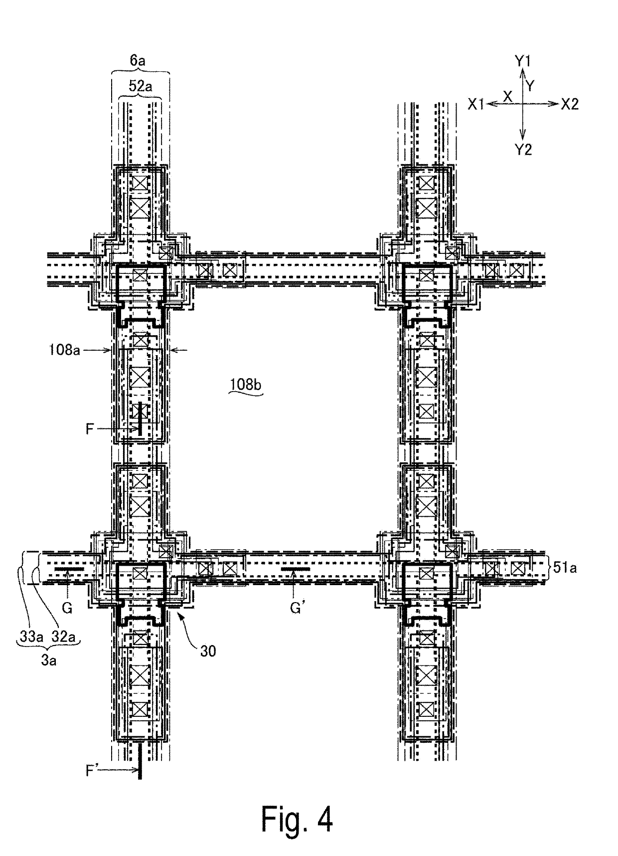
[0118]FIG. 17 is an explanatory diagram of the first substrate 10 used in the electro-optical device 100 according to Exemplary Embodiment 2 of the invention, and corresponds to the cross section G-G′ illustrated in FIG. 4. Note that basic configurations in this exemplary embodiment are the same as in Exemplary Embodiment 1, and thus, common portions are denoted by the same reference signs and a description of the common portions will be omitted. In Exemplary Embodiment 1, the first section 8a1 of the second electrode 8a is provided over both the first hole 17d6 and the second hole 17d7. In this exemplary embodiment, as illustrated in FIG. 17, on the first edge portion 17d1 side of the first contact hole 17d, the first section 8a1 is provided on both the first hole 17d6 and the second hole 17d7, but on the second edge portion 17d2 side, the first section 8a1 is provided only on the first hole 17d6 and is not provided on the second hole 17d7. The rest of the configuration is the same...
exemplary embodiment 3
[0120]FIG. 18 is an explanatory diagram of the first substrate 10 used in the electro-optical device 100 according to Exemplary Embodiment 3 of the invention, and corresponds to the cross section G-G′ illustrated in FIG. 4. Note that basic configurations in this exemplary embodiment are the same as in Exemplary Embodiment 1, and thus, common portions are denoted by the same reference signs and a description of the common portions will be omitted. In Exemplary Embodiment 1, the first contact hole 17d includes the first hole 17d6 and the second hole 17d7 that is slightly larger than the first hole 17d6. In contrast, in this exemplary embodiment, as illustrated in FIG. 18, a section corresponding to the second hole 17d7 is formed so as to extend over a wide region on one side with respect to the first contact hole 17d, in addition to a region overlapping in a plan view with the first hole 17d6.
[0121]Thus, on the surface of the first insulating film 17 on the opposite side to the first ...
exemplary embodiment 4
[0124]FIG. 19 is an explanatory diagram of the first substrate 10 used in the electro-optical device 100 according to Exemplary Embodiment 4 of the invention, and corresponds to the cross section G-G′ illustrated in FIG. 4. FIG. 20 is a process cross-sectional view illustrating a process for forming the terminal 102 and the like on the first substrate 10 illustrated in FIG. 19. The display region 10a and the terminal region 10e are illustrated in FIG. 20. Note that basic configurations in this exemplary embodiment are the same as in Exemplary Embodiment 1, and thus, common portions are denoted by the same reference signs and a description of the common portions will be omitted.
[0125]In Exemplary Embodiment 1, the pixel electrode 9a is configured by a single layer of the electrically conducting film. In contrast, in this exemplary embodiment, as illustrated in FIG. 19, the pixel electrode 9a includes a first electrically conducting film 91a that is made of an ITO film or the like, an...
PUM
 Abstract
Description
Claims
Application Information
 - R&D
- Intellectual Property
- Life Sciences
- Materials
- Tech Scout
- Unparalleled Data Quality
- Higher Quality Content
- 60% Fewer Hallucinations
Browse by: Latest US Patents, China's latest patents, Technical Efficacy Thesaurus, Application Domain, Technology Topic, Popular Technical Reports.
© 2025 PatSnap. All rights reserved.Legal|Privacy policy|Modern Slavery Act Transparency Statement|Sitemap|About US| Contact US: help@patsnap.com


