Active matrix LED display
a led display and active matrix technology, applied in the field of large-area displays, can solve the problems of no large-scale display technology present, no large-scale display technology can find widespread use, and the trend toward a larger-scale display in digital signage has been progressing slowly, so as to minimize the increase in manufacturing costs, enlarge the whole display, and economic efficiency.
- Summary
- Abstract
- Description
- Claims
- Application Information
AI Technical Summary
Benefits of technology
Problems solved by technology
Method used
Image
Examples
example 1
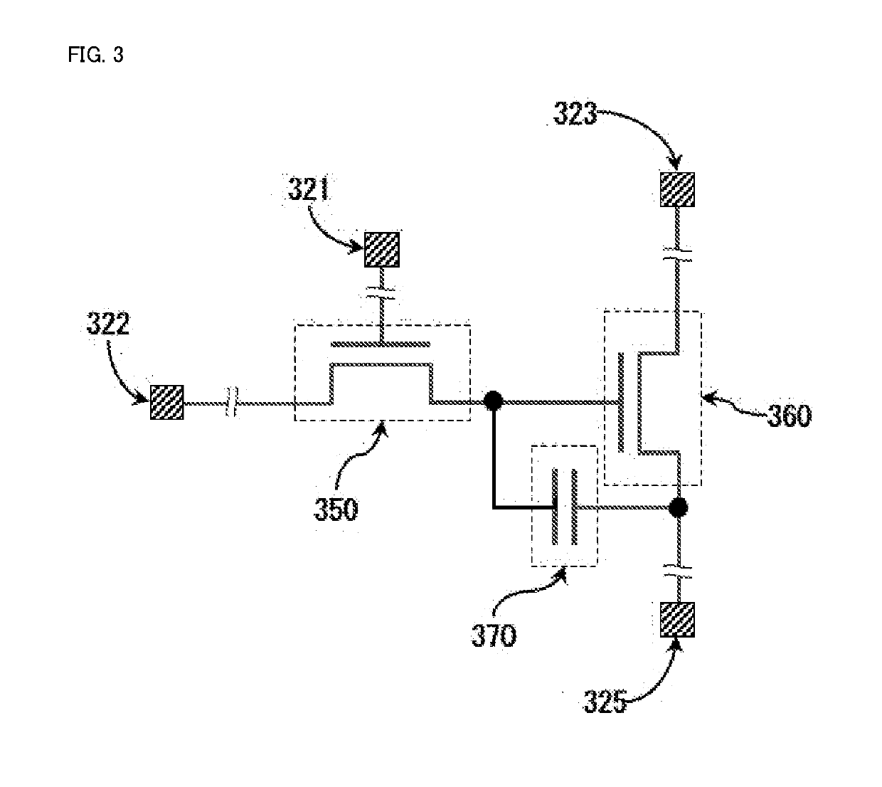
[0034]In the present embodiment, a description will be given to an example in which a display with a size of 2.88 m×1.62 m (pixel size 3 mm×3 mm) in QHD standard is formed as for digital signage by a technology of manufacturing an active matrix type inorganic LED display including a pixel driving circuit using an organic TFT as each light emitting element provided therein with an inorganic LED element of each color of RGB as a light emitting element.
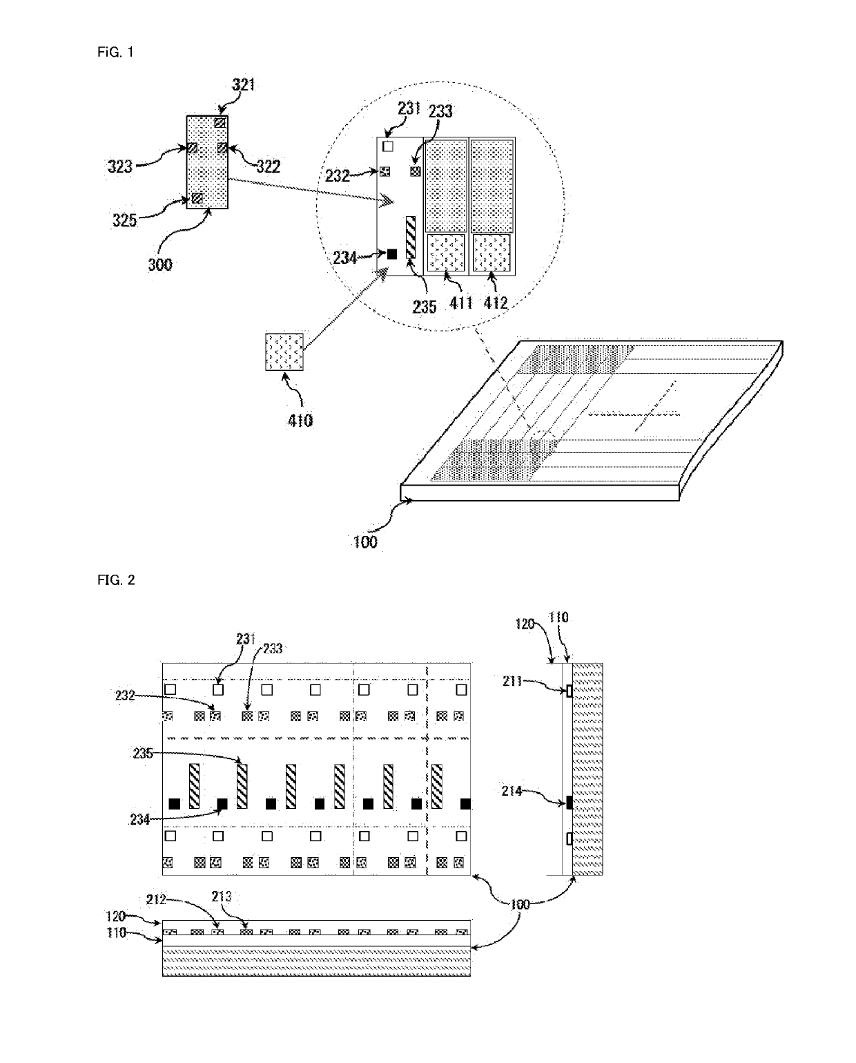
[0035]FIG. 1 shows the basic concept of the present invention, and shows the manner of mounting a pixel driving circuit substrate 300 for each of three colors in each pixel of a substrate 100 of the display main body, and surface mounting inorganic LEDs 410, 411, and 412 of respective colors of RGB. On the display substrate 100, at the stage of mounting a pixel driving circuit substrate, and inorganic LEDs, a row selection line, a column selection line, a power supply line, and a ground line, and pads 231, 232, 233, and 234 electrically ...
example 2
[0041]Then, a description will be given to Second Embodiment for executing the present invention.
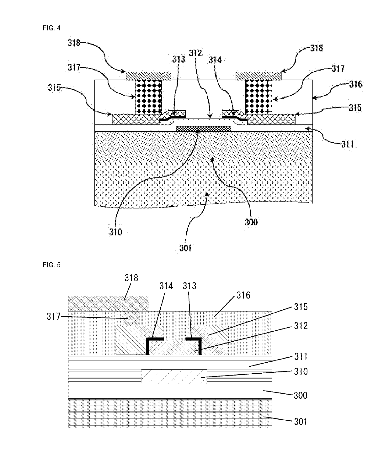
[0042]In accordance with the present embodiment, as shown in First Embodiment for executing the present invention, on a first substrate, a pixel driving circuit including an organic semiconductor thin film is formed; an inorganic LED element is formed on a second substrate by an inorganic semiconductor process; wires and terminal pattern are formed on a third substrate by various printing methods, a photolithography method, or the like; and the first substrate and the second substrate are bonded together, and mounted onto a prescribed part on the third substrate; as a result, an active matrix LED display is manufactured. The difference from the First Embodiment resides in that mounting is achieved by face up in contrast to face down.
[0043]Then, Second Embodiment for executing the present invention will be described in detail.
[0044]First, the pixel driving circuit substrate 300 (FIG. 5) f...
PUM
 Abstract
Description
Claims
Application Information


