Capacitive load driving circuit and image forming apparatus

Active Publication Date: 2019-09-19
FUJIFILM BUSINESS INNOVATION CORP
View PDF0 Cites 0 Cited by
  • Summary
  • Abstract
  • Description
  • Claims
  • Application Information

AI Technical Summary

Benefits of technology

The present invention relates to a circuit for driving a capacitive load. The circuit includes four switching elements and voltage dropper elements that control the flow of electric current through different paths. The technical effect of this circuit is to reduce the number of components and control burden when compared to a circuit that sequentially switches over individual transistors or a circuit for charging a capacitor. The circuit allows for efficient and controllable power supply and prevents rise in temperature by switching between a power supply and a regenerative capacitor.

Problems solved by technology

For reducing power consumption and preventing rise in temperature by switching between a power supply and a regenerative capacitor, it may be necessary to provide a circuit for switching, resulting in increasing the number of components and control burden.
However, aspects of the non-limiting embodiments are not required to overcome the disadvantages described above, and aspects of the non-limiting embodiments of the present disclosure may not overcome any of the disadvantages described above.

Method used


Image

  • Capacitive load driving circuit and image forming apparatus
  • Capacitive load driving circuit and image forming apparatus
  • Capacitive load driving circuit and image forming apparatus

Examples


first modified example

dback Circuit

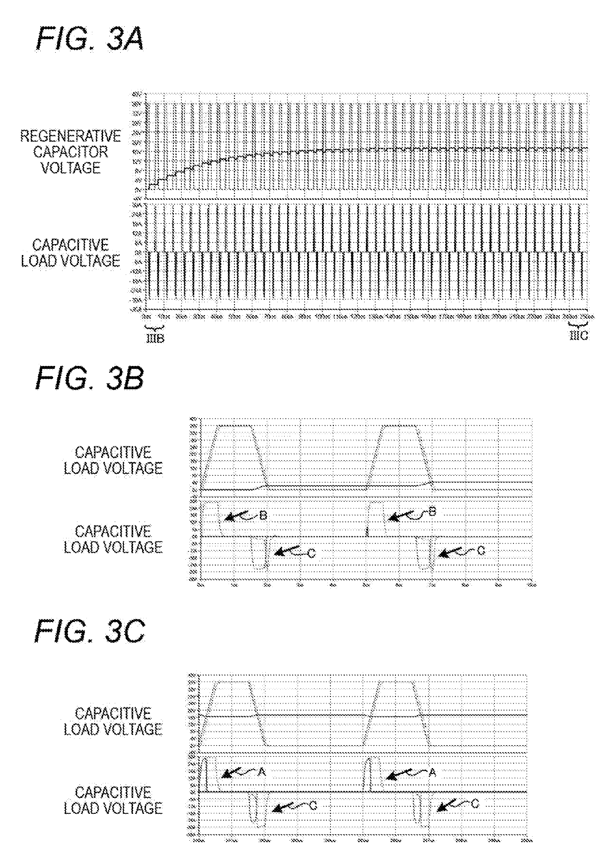
[0080]In the embodiment, the signal line for negative feedback of the voltage driving the capacitive load 200. However, as shown in FIG. 5, when the accuracy achieved by negative feedback is not necessary or a feedforward control is adopted in which a control signal Vin is corrected in advance so as to obtain a target waveform, a capacitive load driving circuit 202A having no signal line for negative feedback may be adopted.

[0081]In the capacitive load driving circuit diagram shown in FIG. 2, the first voltage dropper element 216 and the second voltage dropper element 218 each include the two diodes. In a capacitive load driving circuit diagram shown in FIG. 5, however, a first voltage dropper element 216 and a second voltage dropper element 218 each include a single diode. The reason that the single diode is used is that compared with the capacitive load driving circuit 202 shown in FIG. 2 in which the negative feedback circuit is provided, in the capacitive load drivi...

second modified example 2

r

[0083]In the exemplary embodiment (see FIG. 2), the MOSFET is used as the switching elements 212. More specifically, the n type MOSFET is used for the first switching element 212A and the second switching element 212B. Then, the capacitive load is charged through the second charging path C2 by way of the switching element 212B preferentially by the first voltage dropper element 216 while the potential of the capacitive load is lower than the potential of the capacitor. The p type MOSFET is used for the third switching element 212C and the fourth switching element 212D. Then, the capacitive load is discharged through the second discharging path D2 by way of the fourth switching element 212D preferentially by the second voltage dropper element 218 while the potential of the capacitive load is higher than the potential of the capacitor.

[0084]In contrast, a bipolar transistor is used as a switching element 230 in a capacitive load driving circuit 202B according to a second modified exa...

third modified example

[0094]FIG. 7 shows a capacitive load driving circuit 202C in which a capacitive load 200 has a minus voltage as a third modified example. In the case of this capacitive load driving circuit 202C, the supply voltage of the capacitive load driving circuit 202 according to the embodiment should be reversed to a minus side.

[0095]In this case, as in the capacitive load driving circuit 202 according to the embodiment, when a differential amplifier is connected as a non-reversible amplifier, the differential amplifier is also caused to operate to the minus side. Thus, for example, assuming that an input of the differential amplifier is connected to a digital-to-analogue (DA) converter, when the differential amplifier is a rail-to-rail differential amplifier, the DA converter may be driven at 5V, whereby a level conversion with a logic is facilitated.

[0096]Then, in the capacitive load driving circuit 202C according to the third modified example, the differential amplifier is configured as a...


PUM


Abstract

A capacitive load driving circuit includes a first switching element, a second switching element, a third switching element, a fourth switching element and voltage dropper elements. The first switching element is provided on a first charging path extending from a power supply to a capacitive load. The second switching element is provided on a second charging path extending from a capacitor to the capacitive load. The third switching element is provided on a first discharging path extending from the capacitive load to a ground. The fourth switching element is provided on a second discharging path extending from the capacitive load to the capacitor. The voltage dropper elements are provided on each of control signal power supply paths to the first switching element, to the second switching element, to the third switching element and to the fourth switching element. The voltage dropper elements are configured to make electric current flow more easily through the second charging path than through the first charging path when charging the capacitive load and to make electric current flow more easily through the second discharging path than through the first discharging path when discharging the capacitive load by a potential difference.

Description

CROSS REFERENCE TO RELATED APPLICATION[0001]This application is based on and claims priority under 35 USC 119 from Japanese Patent Application No. 2018-051676 filed Mar. 19, 2018.BACKGROUNDTechnical Field[0002]The present invention relates to a capacitive load driving circuit and an image forming apparatus.Related Art[0003]JP-A-H11-170529 discloses providing a regenerative capacitor in addition to a capacitive load. The regenerative capacitor is charged when performing discharging of the capacitive load, and discharged when performing charging of the capacitive load for recovering energy to reduce energy consumption.[0004]JP-A-2006-256149 discloses charging a capacitive load using two different voltage levels by switching between series and parallel connection with a switch for switching between two capacities, and recovering energy by charging the two capacities when performing discharging of the capacitive load.SUMMARY[0005]For reducing power consumption and preventing rise in tem...

Claims


Application Information

Patent Timeline
IPC IPC(8): B41J2/045H03K17/687H03K4/94
CPCH03K17/667H03F3/45071B41J2/04555B41J2/04541B41J2/04581H03K4/94H03K17/6872B41J2/0457B41J2/01B41J2/11B41J29/38B41J2/04548H03F3/2173H03F2200/297
Inventor IKEDA, CHIKAHO
Owner FUJIFILM BUSINESS INNOVATION CORP
Why Eureka
Try Eureka