

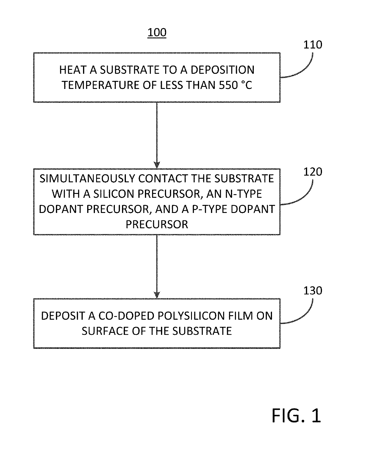
Method of depositing a co-doped polysilicon film on a surface of a substrate within a reaction chamber
a technology of polysilicon film and reaction chamber, which is applied in the direction of semiconductor devices, semiconductor/solid-state device details, electrical equipment, etc., can solve the problems of unwanted material formation, unfavorable conventional device scaling, and material thermal diffusion into unfavorable areas of the device structur
- Summary
- Abstract
- Description
- Claims
- Application Information
AI Technical Summary
Benefits of technology
Problems solved by technology
Method used
Image

Examples
Embodiment Construction
[0013]Although certain embodiments and examples are disclosed below, it will be understood by those in the art that the invention extends beyond the specifically disclosed embodiments and / or uses of the invention and obvious modifications and equivalents thereof. Thus, it is intended that the scope of the invention disclosed should not be limited by the particular disclosed embodiments described below.
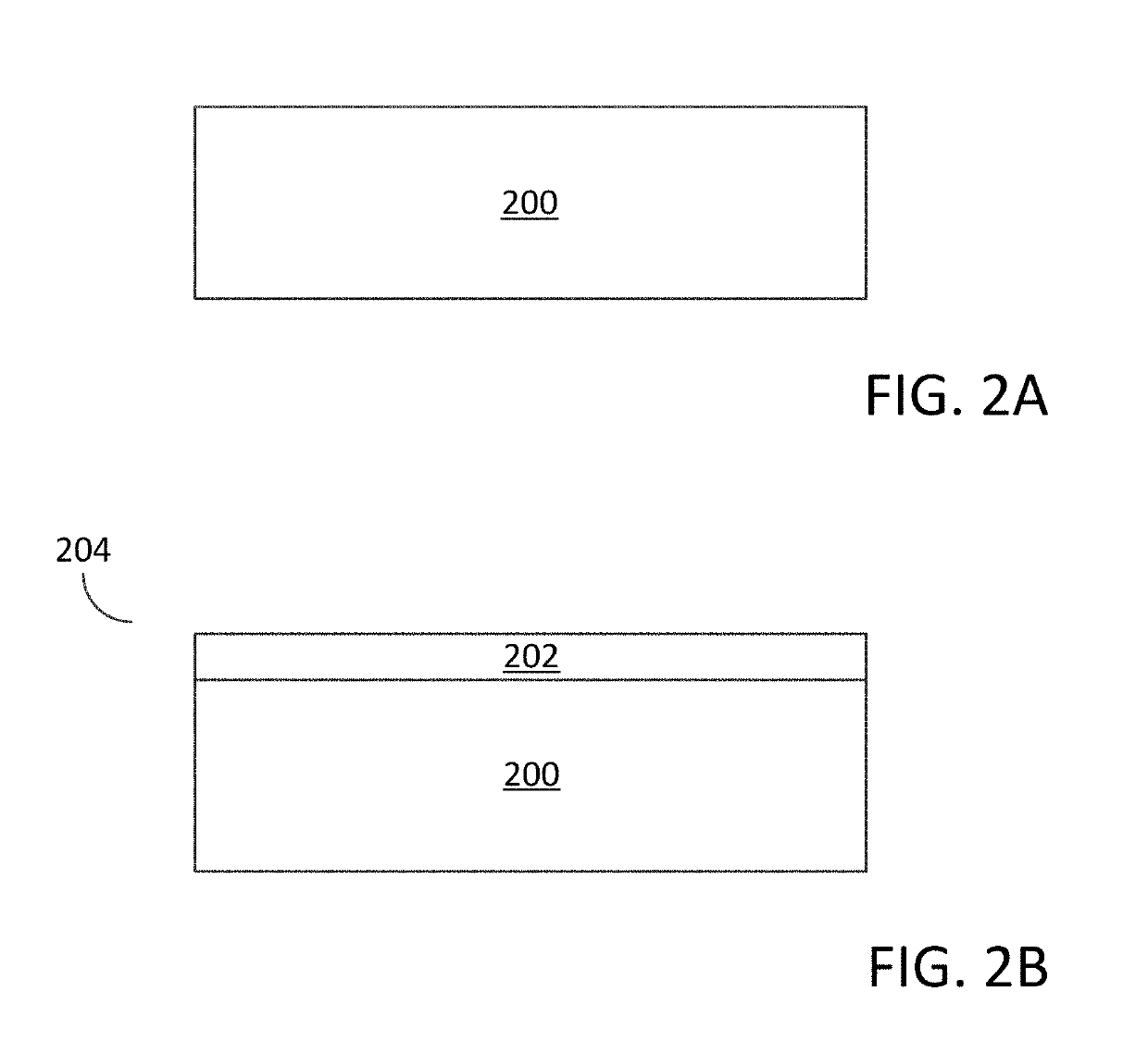
[0014]As used herein, the term “substrate” may refer to any underlying material or materials that may be used, or upon which, a device, a circuit or a film may be formed.
[0015]As used herein, the term “chemical vapor deposition” or “CVD” may refer to a process wherein a substrate is exposed to one or more volatile precursors, which react and / or decompose on a substrate surface to produce a desired deposition. CVD processes are distinct from alternative deposition methods, such as, for example, molecular beam epitaxy (MBE), or atomic layer deposition (ALD).
[0016]As used herein, the term...
PUM
 Abstract
Description
Claims
Application Information