

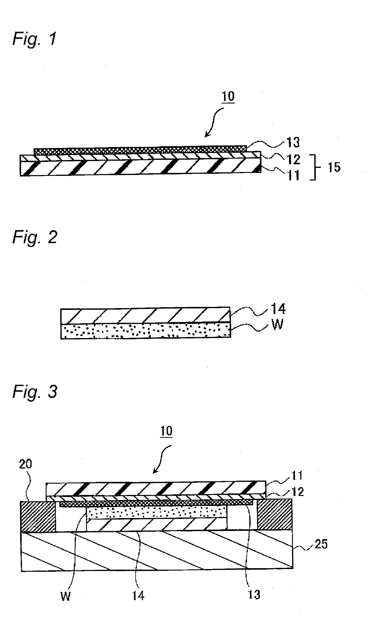
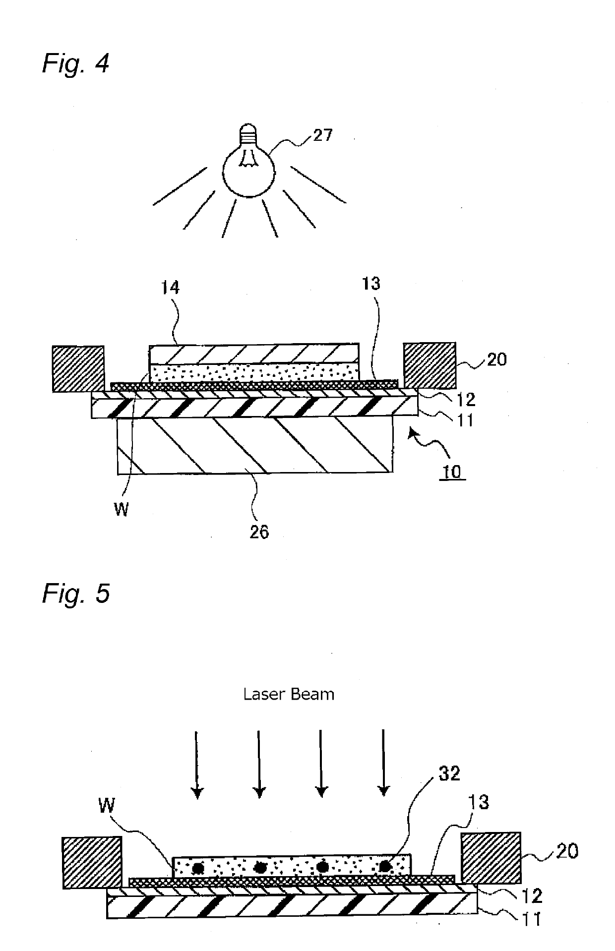
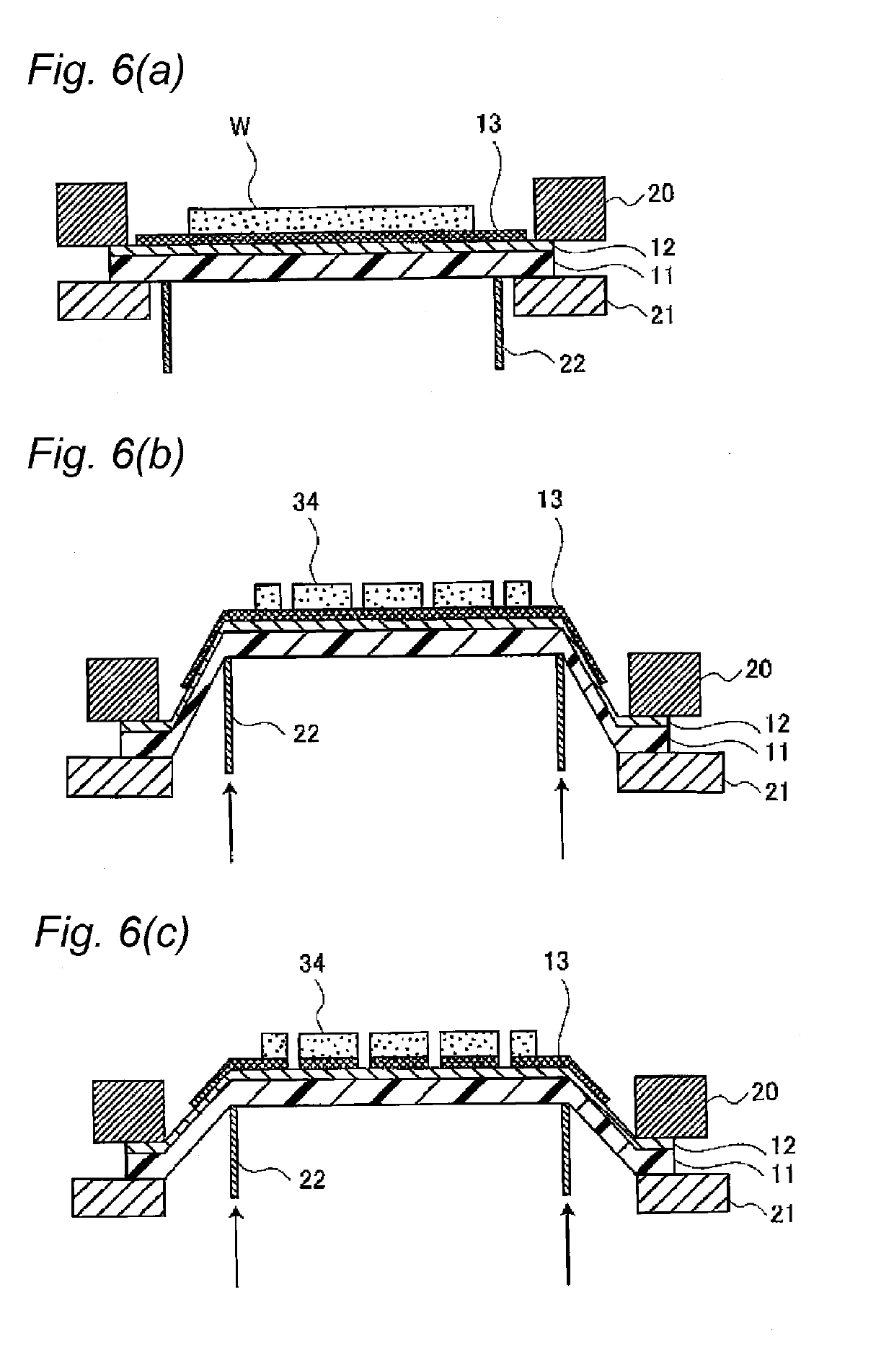
Semiconductor-processing tape
- Summary
- Abstract
- Description
- Claims
- Application Information
AI Technical Summary
Benefits of technology
Problems solved by technology
Method used
Image

Examples
example 1
[0275]To the release-treated surface of a release liner composed of a polyethylene-terephthalate film one surface of which has been subjected to a release treatment, the removable adhesive composition was coated so that a thickness after drying would be 10 μm. After drying it at 110° C. for 2 minutes, the coated composition was laminated on the base material film 1, to prepare a removable adhesive sheet having a removable adhesive layer formed on the base material film 1.
[0276]Next, to the release-treated surface of another release liner composed of a polyethylene-terephthalate film one surface of which has been subjected to a release treatment, the adhesive composition (b-1) was coated so that a thickness after drying would be 60 μm. Drying it at 130° C. for 3 minutes, an adhesive film having an adhesive layer formed on the release liner was prepared.
[0277]Next, the removable adhesive sheet was cut into a circle of the size enough to allow the circle to laminate on a ring frame so ...
example 2
[0278]The semiconductor-processing tape 2 was prepared by the same materials and manner as in Example 1, except for using the base material film 2 as a base material film. A layer composed of the non-crosslinked resin B of the base material film 2 was laminated on the dried removable adhesive composition.
example 3
[0279]The semiconductor-processing tape 3 was prepared by the same materials and manner as in Example 1, except for using the base material film 3 as a base material film. The 10 μm-thick layer side of the two layers composed of the ionomer resin A of the base material film 3 was laminated on the removable adhesive layer.
PUM
| Property | Measurement | Unit |
|---|---|---|
| Temperature | aaaaa | aaaaa |
| Length | aaaaa | aaaaa |
| Pressure | aaaaa | aaaaa |
Abstract
Description
Claims
Application Information