Optoelectronic device with light-emitting diodes

a technology of light-emitting diodes and optoelectronic devices, which is applied in the direction of semiconductor devices, basic electric elements, electrical apparatus, etc., can solve the problems of poor internal quantum efficiency of light-emitting diodes comprising three-dimensional elements emitting a red light, and poor internal quantum efficiency of known materials used to form micrometer-range photoluminescent particles, and achieve high internal quantum efficiency and high internal quantum efficiency. , the effect of high internal quantum

Active Publication Date: 2019-10-17
ALEDIA
View PDF8 Cites 7 Cited by
  • Summary
  • Abstract
  • Description
  • Claims
  • Application Information

AI Technical Summary

Benefits of technology

[0011]Another object of an embodiment is that all the light-emitting diodes of the optoelectronic device show high internal quantum efficiency.
[0012]Another object of an embodiment is that the photoluminescent blocks of the optoelectronic device show high internal quantum efficiency.
[0013]Another object of an embodiment is for optoelectronic devices comprising light-emitting diodes to be capable of being manufactured at an industrial scale and at a low cost.

Problems solved by technology

However, known light-emitting diodes comprising three-dimensional elements emitting a red light show poor internal quantum efficiency.
However, known materials used to form micrometer-range photoluminescent particles show poor internal quantum efficiency.

Method used


Image

  • Optoelectronic device with light-emitting diodes
  • Optoelectronic device with light-emitting diodes
  • Optoelectronic device with light-emitting diodes

Examples


Embodiment Construction

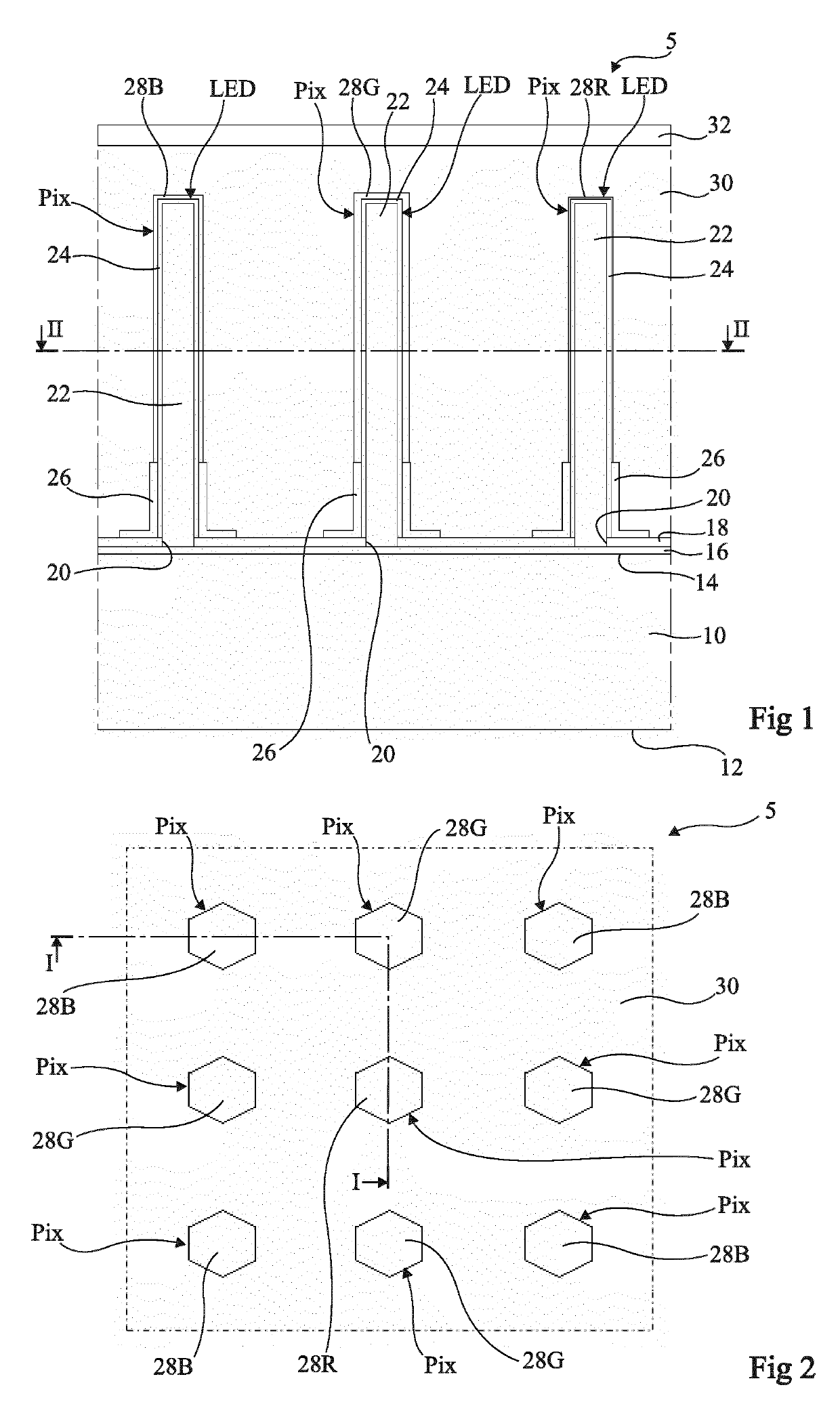
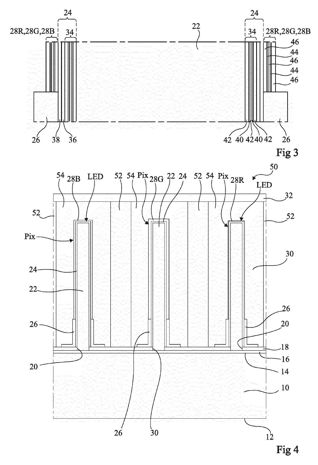
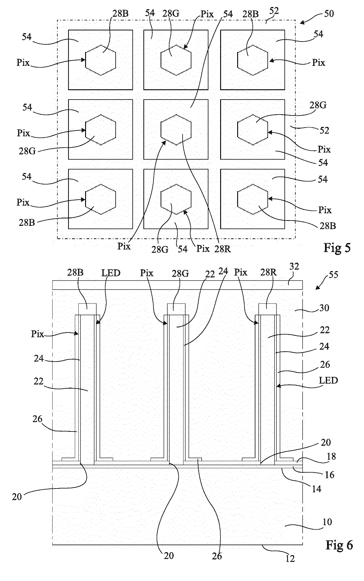
[0039]For clarity, the same elements have been designated with the same reference numerals in the various drawings and, further, as usual in the representation of electronic circuits, the various drawings are not to scale. Further, only those elements which are useful to the understanding of the present description have been shown and will be described. In particular, the means for biasing a light-emitting diode of an optoelectronic device are well known and will not be described.

[0040]The present description relates to optoelectronic devices comprising light-emitting diodes formed from three-dimensional elements, for example, microwires or nanowires. In the following description, embodiments are described for light-emitting diodes formed from microwires or nanowires. However, these embodiments may be implemented for three-dimensional elements other than microwires or nanowires, for example, pyramid-shaped three-dimensional elements.

[0041]In the following description, unless otherwi...


PUM


Abstract

An optoelectronic device including light-emitting diodes (LED), each light-emitting diode including a semiconductor element corresponding to a nanowire, a microwire, and/or a nanometer- or micrometer-range pyramidal structure, and a shell at least partially covering the semiconductor element and adapted to emit a radiation and for each light-emitting diode, a photoluminescent coating including a single quantum well, multiple quantum wells or an heterostructure, covering at least part of the shell and in contact with the shell or with the semiconductor element and adapted to convert by optical pumping the radiation emitted by the shell into another radiation.

Description

[0001]The present patent application claims the priority of the French patent application FR16 / 63507 which will be considered as an integral part of the present description.BACKGROUND[0002]The present disclosure relates to an optoelectronic device, particularly a display screen or an image projection device, comprising light-emitting diodes formed by three-dimensional elements, particularly semiconductor microwires or nanowires.Discussion of the Related Art[0003]A pixel of an image corresponds to the unit element of the image displayed by the optoelectronic device. When the optoelectronic device is a color image display optoelectronic device, it generally comprises for the display of each pixel of the image at least three components, also called display sub-pixels, which each emit a light radiation substantially in a single color (for example, red, green, and blue). The superposing of the radiations emitted by the three display sub-pixels provides the observer with the color sensati...

Claims


Application Information

Patent Timeline
Patent Type & Authority Applications(United States)
IPC IPC(8): H01L27/15H01L33/24H01L33/50H01L33/08H01L33/56
CPCH01L2933/005H01L27/156H01L33/504H01L2933/0041H01L33/56H01L33/18H01L33/505H01L33/24H01L33/08H01L29/15H01L29/0676H01L29/125H10K50/115
Inventor TAN, WEI SINGILET, PHILIPPE
Owner ALEDIA
Why Eureka
Try Eureka