Vertical transition method applied between coaxial structure and microstrip line
a vertical transition and microstrip technology, applied in the field of vertical transition methods, can solve the problems of severe insertion loss of vertical transition at higher frequencies, ineffective reduction of severe insertion loss at higher frequencies, and inability to solve problems, so as to improve vertical signal transmission, improve electromagnetic field transformation, and reduce the effect of insertion loss
- Summary
- Abstract
- Description
- Claims
- Application Information
AI Technical Summary
Benefits of technology
Problems solved by technology
Method used
Image
Examples
second embodiment
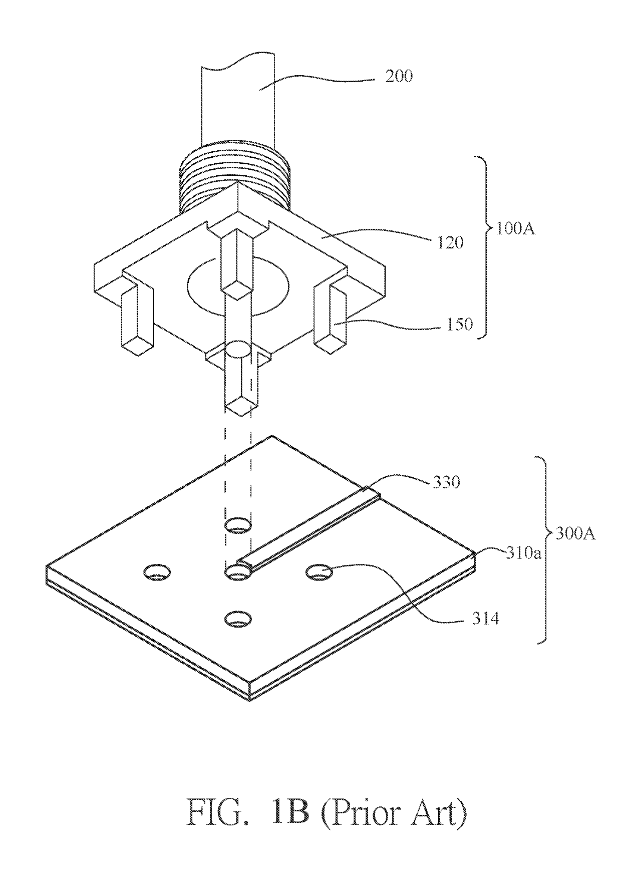
[0057]FIG. 4 is the present invention in which the coaxial connector 100A is placed above the microstrip line 400A. The unwrapped end 130A of the center conductor 130 passes through the transition hole 420 from the upper side 412A of the microstrip line 400, and is soldered to a metallic ring 421 from the ground-plane side 450A of the microstrip line 400 to electrically connect the center conductor 130 to the signal line 430. In FIG. 4, the mounting wall 120 includes four corners 121. To turn a flange-mount coaxial connector 100 into a PCB-mount coaxial connector 100A, four pillars 150 are attached to the mounting wall 120 of the coaxial connector 100A with one pillar 150 connected to each corner 121 of the mounting wall 120 through a base 151 at the end of the pillar 150. The thickness T1 of the base 151 is required to be greater than the thickness T2 of the signal line 430. The substrate 410 of the microstrip line 400A includes a plurality of mounting holes 416 outside the removed...
fourth embodiment
[0066]FIG. 9 shows a method for a top-mounted vertical transition according to the present invention. The substrate 410 of the microstrip line 400D includes four mounting holes 416 outside the removed portion 452 of the ground plane 450, in addition to the technical features shown in FIG. 8. Each of these mounting holes 416 is created for its corresponding pillar 150 under the mounting wall 120 to pass through the substrate 410 and the ground plane 450. And the penetrating end 152 of each pillar 150 is soldered onto the ground plane 450, thereby fixing the coaxial connector 100A above the microstrip line 400D. The base 151 of each pillar 150 is designed to prevent short circuits between the mounting wall 120 and the signal line 430 after final assembly.
[0067]As shown in FIG. 9A, the substrate 410 is characterized by a dielectric constant of 6.15, a thickness of 32 mils, and a size of 30 mm×40 mm. C1 is defined as the center of the removed portion 452, the diameter D1 of the removed ...
PUM
 Abstract
Description
Claims
Application Information


