Optical module
a technology of optical modules and modules, applied in the field of optical modules, can solve the problems of adverse effect on the operation of optical modules, difficulty in appropriately adjusting temperature of thermoelectric elements, and increase in heat generation of integrated semiconductor laser devices
- Summary
- Abstract
- Description
- Claims
- Application Information
AI Technical Summary
Benefits of technology
Problems solved by technology
Method used
Image
Examples
first embodiment
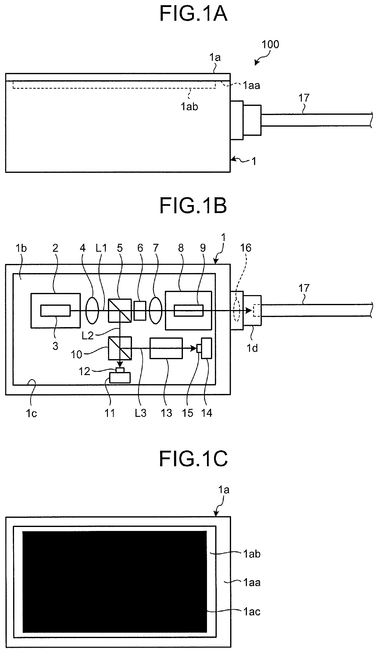
[0019]FIGS. 1A to 1C are schematic diagrams each illustrating a configuration of a semiconductor laser module serving as an optical module according to a first embodiment of the present disclosure. As illustrated in a side view in FIG. 1A, a semiconductor laser module 100 is provided with a housing 1 that includes a lid 1a. As illustrated in FIG. 1B, which is a top view of the semiconductor laser module 100 with the lid 1a removed from the housing 1, the semiconductor laser module 100 includes a submount 2, a laser element 3, a collimator lens 4, a beam splitter 5, an optical isolator 6, a condenser lens 7, a submount 8, an SOA 9, a beam splitter 10, a photodiode (PD) 12 supported by a PD carrier 11, an etalon filter 13, a PD 15 supported by a PD carrier 14, all of which are disposed within the housing 1.
[0020]The housing 1 includes the lid 1a, a bottom plate 1b, and a sidewall portion 1c. The sidewall portion 1c on the right side of FIG. 1B is provided with a holder unit 1d, in whi...
second embodiment
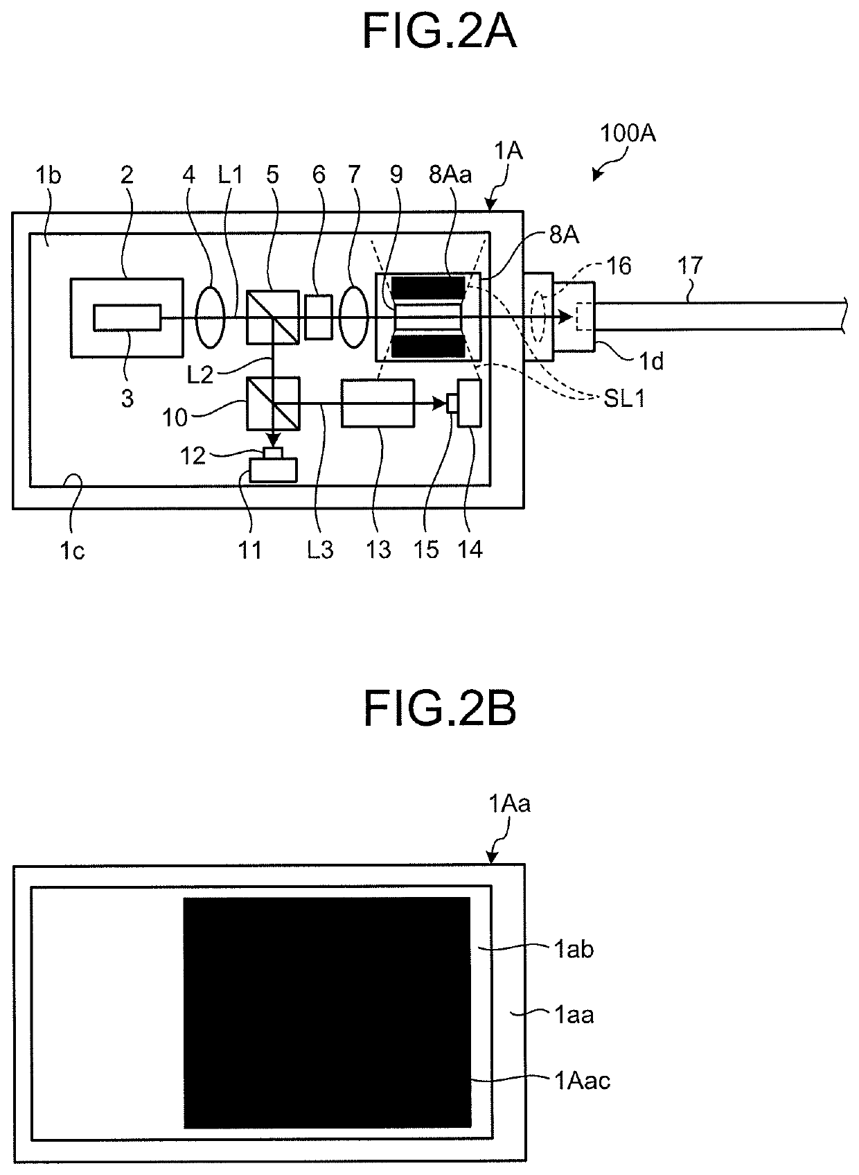
[0050]FIGS. 2A and 2B are schematic diagrams each illustrating a configuration of a semiconductor laser module serving as an optical module according to a second embodiment of the present disclosure. A semiconductor laser module 100A according to the second embodiment has a configuration obtained by replacing the housing 1 with a housing 1A and replacing the submount 8 with a submount 8A in the configuration of the semiconductor laser module 100 according to the first embodiment. The housing 1A has a configuration obtained by replacing the lid 1a of the housing 1 with a lid 1Aa.
[0051]FIG. 2A is a top view of the semiconductor laser module 100A with the lid 1Aa removed from the housing 1A. FIG. 2B is a diagram illustrating an inner surface of the lid 1Aa. In the same way as the submount 8, the submount 8A is made of a material having high thermal conductivity, such as aluminum oxide, aluminum nitride, boron nitride, copper, or silicon. Partial areas of a surface of the submount 8A, t...
third embodiment
[0056]FIG. 4 is a schematic diagram illustrating a configuration of a semiconductor laser module serving as an optical module according to a third embodiment of the present disclosure, and is a top view of the semiconductor laser module with a lid removed. A semiconductor laser module 100B according to the third embodiment has a configuration obtained by replacing the housing 1A with a housing 1B and replacing the submount 2 with a submount 2B in the configuration of the semiconductor laser module 100A according to the second embodiment. The housing 1B has a configuration obtained by replacing the sidewall portion 1c of the housing 1A with a sidewall portion 1Bc.
[0057]In the same way as the submount 2, the submount 2B is made of a material having high thermal conductivity, such as aluminum oxide, aluminum nitride, boron nitride, copper, or silicon. A partial area of a surface of the submount 2B, that is, a rear side of an area in which the laser element 3 is to be placed (a side of ...
PUM
 Abstract
Description
Claims
Application Information


