Coupled-inductor Based Resonator And Formed Voltage Controlled Oscillator Thereof

a voltage control and oscillator technology, applied in the field of voltage control oscillators, can solve the problems of increasing cost and complexity, negative impact on reliability and robustness, etc., and achieve the effects of reducing voltage swing, and reducing cost and complexity

Active Publication Date: 2019-12-05
CHENGDU SICORE SEMICON CORP LTD
View PDF3 Cites 1 Cited by
  • Summary
  • Abstract
  • Description
  • Claims
  • Application Information

AI Technical Summary

Benefits of technology

[0007]In some embodiments, the multi-band VCO features a coupled-inductor based resonator. The resonator comprises a primary path and a secondary path inductively coupled to the primary path. The primary path comprises multiple LC tuning stages coupled in series with each stage having an adjustable capacitor (e.g. a varactor or a back-to-back varactor pair) and a primary inductor inductively coupled to the secondary path. The secondary path comprises multiple secondary inductors inductively coupled to respective primary inductors in the primary path. Furthermore, the secondary path comprises a plurality of controllable switches which are controlled to switch ON or OFF simultaneously to engage / disengage the inductive coupling between the primary path and the secondary path. The number of the switches may or may not be the same as the inductors in the secondary path. Through switching ON or OFF all the switches simultaneously in the secondary path, the equivalent inductance value of each LC tuning stage is varied to act as a switchable inductor. With multiple LC tuning stages in the primary path, the resonator therefore has distributed LC tuning capacity with enhanced frequency tuning range. The capacitor in each LC tuning stage may comprise a variable capacitor, which may be controlled together with the switchable inductor to form multiple tuning bands. The tuning bands may have overlaps such that the overall frequency tuning range of the VCO has no gap.
[0008]Incorporating multiple LC tuning stages minimizes voltage swing across each tuning stages, thus minimizing phase noise caused by nonlinearity in the resonator. The configuration of multiple switches coupled in series in the secondary path allows relatively large switch size for each switch to achieve small ON resistance (RON) for each stage during switch ON period and large overall OFF resistance (ROFF) during switch OFF period such that the primary path is less affected in the OFF period. Furthermore, multiple switches coupled in series reduces voltage swing across each switch in the secondary path, thus reducing phase noise caused by nonlinearity of those switches.
[0009]In some embodiments, the multi-band VCO may be configured as a push-push VCO to further reduce oscillator phase noise as compared to conventional VCO. The push-push VCO comprises a first oscillator and a second oscillator coupled in a push-push configuration to output a single-ended or a differential output signal to an amplifier. The abovementioned configurations for the multi-band VCO are also applicable to the first and second oscillators. The push-push configuration may be symmetric along a virtue ground or a true ground. The amplifier may be a single-ended buffer amplifier or a differential amplifier depending on the output signal. Alternatively, the multi-band VCO may output a differential output signal to a doubler for doubling the output signal frequency band.

Problems solved by technology

Using multiple VCOs for multiple frequency bands may bring many undesirable issues, such as increasing cost and complexity, negative impact on reliability and robustness, etc.

Method used


Image

  • Coupled-inductor Based Resonator And Formed Voltage Controlled Oscillator Thereof
  • Coupled-inductor Based Resonator And Formed Voltage Controlled Oscillator Thereof
  • Coupled-inductor Based Resonator And Formed Voltage Controlled Oscillator Thereof

Examples


embodiment 1

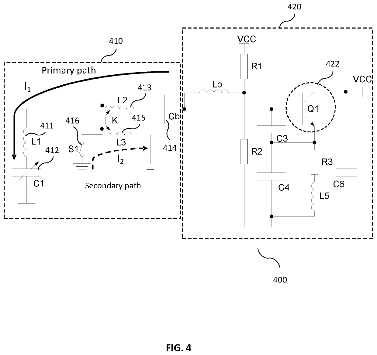
[0028]FIG. 4 is a circuit diagram of a multi-band VCO according to embodiment 1 of the invention. As shown in FIG. 4, the multi-band VCO 400 comprises a resonator 410 and a negative resistance circuit 420. The resonator 410 is a coupled-inductor based resonator comprising a primary path and a secondary path inductively coupled to the primary path. The resonator 410 incorporates a first LC tuning stage (comprising inductor L1 411 and capacitor C1 412), a coupled-inductor tuning stage (comprising inductor L2 413 and the secondary path) and a capacitor Cb 414 for DC or low frequency isolation. The coupled-inductor tuning stage inductively couples to the secondary path. The secondary path comprises a controllable switch S1 416 and a secondary inductor L3 415 inductively coupled to inductor L2 413 in the primary path. The controllable switch S1 416 may be controlled to switch ON or OFF to engage / disengage the inductive coupling between inductor L2 on the primary path and inductor L3 on t...

embodiment 2

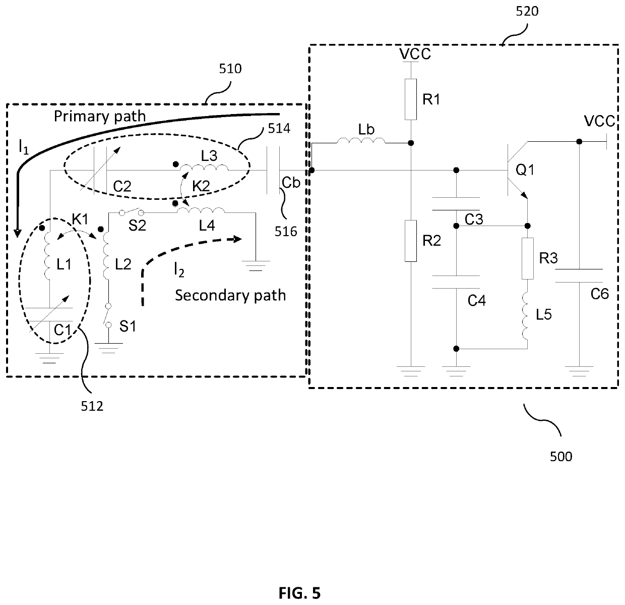
[0035]FIG. 5 is a circuit diagram of a VCO 500 with multiple switches in secondary path according to embodiment 2 of the invention. Similar to the VCO 400 shown in FIG. 4, the VCO 500 also comprises a coupled-inductor based resonator 510 comprising a primary path and a secondary path inductively coupled to the primary path. Different from the primary path in resonator 410, the primary path in resonator 510 comprises multiple LC tuning stages coupled in series, e.g. a first LC tuning stage 512 comprising a first inductor L1 and a first capacitor C1, a second LC tuning stage 514 comprising a second inductor L3 and a second capacitor C2. The inductor of each LC tuning stage is inductively coupled to a respective secondary inductor in the secondary path. For example, the first inductor L1 inductively couples to a first secondary inductor L2 and the second inductor L3 inductively couples to a second secondary inductor L4. Capacitors C1 and C2 may be one or more fixed capacitor, one or mo...

embodiment 3

[0040]In some embodiments, the multi-band VCO may be configured as a push-push VCO to further reduce oscillator phase noise as compared to conventional VCO. FIG. 6 is a multi-band push-push VCO 600 according to embodiment 3 of the invention. The push-push VCO 600 is formed by having two single-ended VCO 610 and 620 implemented in a balanced structure. The single-ended VCOs 610 and 620 couple in a balanced structure symmetrically along a symmetric line 660, which may be a virtual ground. The output signal from location 630 of the push-push VCO is fed to a single-ended buffer amplifier A1640 via a capacitor Cd 632 to generate an amplified output signal 642. Due to the push-push VCO structure, output signal from location 630 (or from other points along virtual GND, e.g., connection point between C1 and C1′) naturally cancel odd harmonics and amplify even harmonics, output location 630 is naturally a good location to tap output an output signal with doubled signal frequency of resonance...


PUM


Abstract

Various embodiments of the invention relate to a Multi-Band Voltage Controlled Oscillator (VCO). The multi-band VCO features a coupled-inductor based resonator. The resonator comprises a primary path and a secondary path inductively coupled to the primary path. The primary path comprises multiple LC tuning stages coupled in series with each stage having an adjustable capacitor and a primary inductor inductively coupled to the secondary path. The secondary path comprises multiple secondary inductors inductively coupled to respective primary inductors in the primary path. Furthermore, the secondary path comprises a plurality of controllable switches which are controlled to switch ON or OFF simultaneously to engage/disengage the inductive coupling between the primary path and the secondary path. Incorporating multiple LC tuning stages lowers voltage swing across each tuning stages, thus minimizing phase noise caused by nonlinearity in the resonator.

Description

BACKGROUNDA. Technical Field[0001]The present invention relates generally to a voltage controlled oscillator, and more particularly to a multi-band voltage controlled oscillator.B. Background of the Invention[0002]A voltage-controlled oscillator (VCO) is an electronic oscillator with oscillation frequency controlled by an input voltage. The applied input voltage determines the instantaneous oscillation frequency. A VCO may be used for various applications, e.g. frequency modulation (FM), phase modulation (PM), a phase-locked loop, etc.[0003]A VCO may comprise a resonator with an amplifier to prevent the amplitude from decaying and isolate the resonator from the output such that the load does not affect the resonator. The resonator may be an inductor-capacitor (LC) oscillator with its resonating frequency variable in response to a control voltage. A semiconductor diode (e.g. varactor) having a voltage-dependent capacitance can be used to change the frequency of an oscillator by varyi...

Claims


Application Information

Patent Timeline
Patent Type & Authority Applications(United States)
IPC IPC(8): H03B5/12
CPCH03B5/1243H03B2200/009H03B5/1218H03B5/1293H03B5/1231H03B5/1262H03B5/1265H03H7/09H03B5/1203H03B5/1268
Inventor ZHANG, CEMIN
Owner CHENGDU SICORE SEMICON CORP LTD
Why Eureka
Try Eureka