Display panel and display device

a display panel and display device technology, applied in the field of display technologies, can solve the problems of large capacitance, affecting the touch sensitivity, and the production of high-quality, high-resolution oled displays still faces many challenges, so as to improve the touch precision of the oled touch screen, and eliminate the effect of area

Active Publication Date: 2019-12-26
WUHAN CHINA STAR OPTOELECTRONICS SEMICON DISPLAY TECH CO LTD
View PDF1 Cites 10 Cited by
  • Summary
  • Abstract
  • Description
  • Claims
  • Application Information

AI Technical Summary

Benefits of technology

[0051]The beneficial effect of the present invention: the present invention eliminates the area without touch-control function on the display panel and improves the touch precision of the OLED touch screen by placing a plurality of conductive lines on one side of the first common electrode plate, by placing the conductive lines and the first common electrode plate on the two film layers respectively, and electrically connecting via the through holes of the insulation layer.

Problems solved by technology

At present, people are increasingly demanding higher level of detail, that is, the resolution, but production of high-quality, high-resolution OLED displays still faces many challenges.
1. The mutual capacitance touch screen has a large capacitance between the electron emission layer (i.e., the cathode) of OLED and touch sensor, resulting in a large capacitance, which affects the sensitivity of the touch.
2. The self-capacitance touch screen (single layer multi-point) divides the entire screen into M*N areas, each area is a separate transparent conductive electrode block, and each transparent conductive electrode block passes the signal line and touch on the same layer. That is, each transparent conductive electrode block independently forms a capacitance to the surrounding environment. When finger approaches a transparent conductive electrode at a certain position, a coupling capacitor is introduced, causing the detected capacitance to increase, and the IC determines that the position is touched. However, since the signal line occupies a part of the touch screen, the touch cannot be achieved at this position. Therefore, the single-layer multi-point self-capacitance touch screen has poor touch precision issues.

Method used


Image

  • Display panel and display device
  • Display panel and display device
  • Display panel and display device

Examples


Embodiment Construction

[0058]In the following detailed description of the preferred embodiments, reference is made to the accompanying drawings which form a part hereof, and in which is shown by way of illustration specific embodiments in which the invention may be practiced. In this regard, directional terminology, such as “top”, “bottom”, “front”, “back”, “left”, “right”, “inside”, “outside”, “side”, etc., is used with reference to the orientation of the figure(s) being described. As such, the directional terminology is used for purposes of illustration and is in no way limiting. Throughout this specification and in the drawings like parts will be referred to by the same reference numerals.

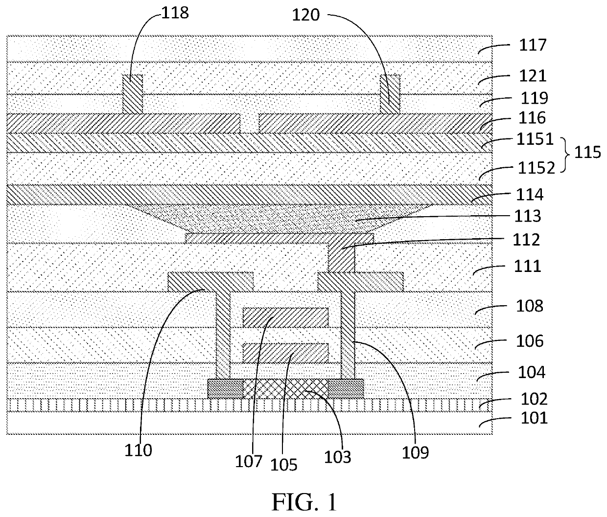
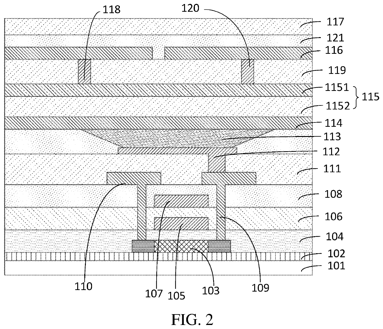
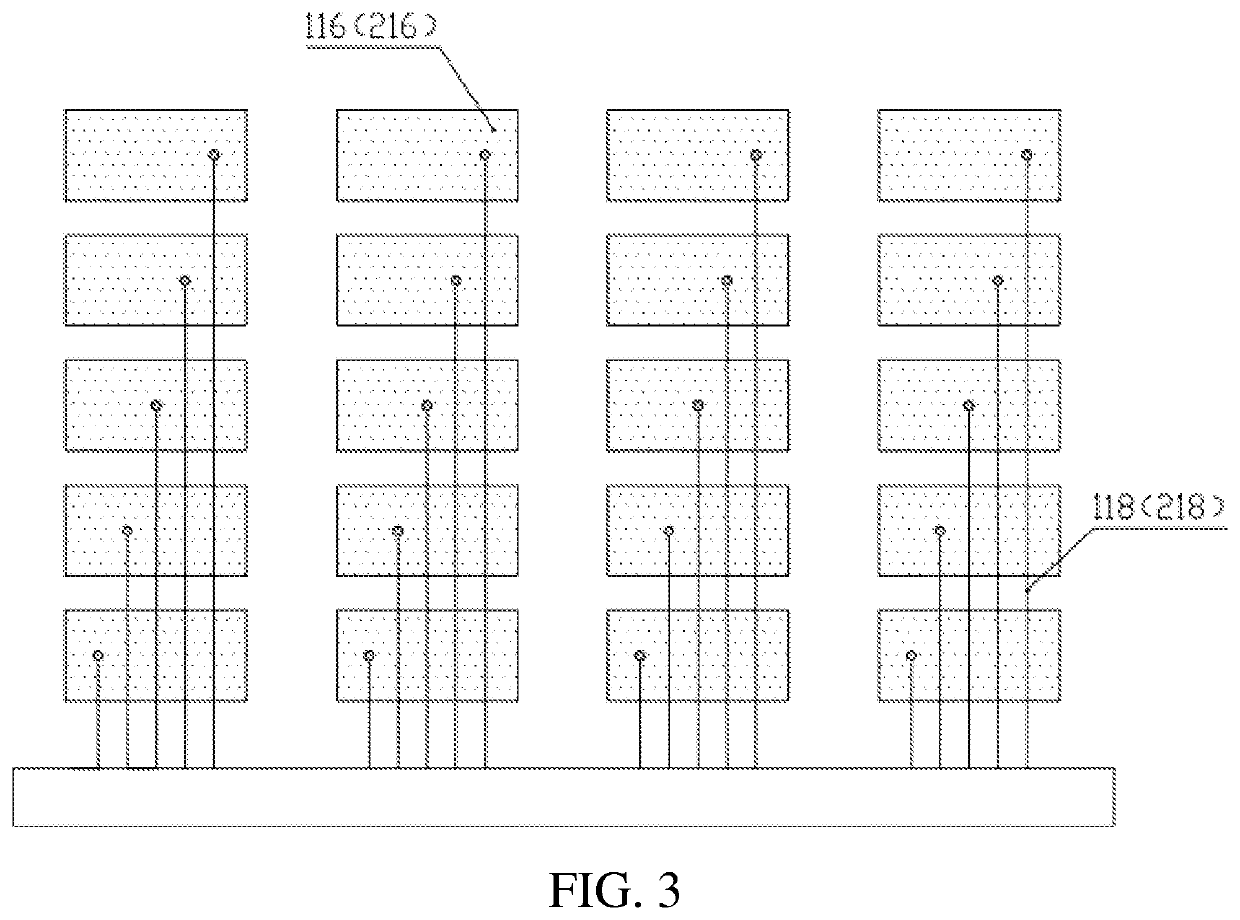
[0059]FIG. 1 shows a display panel of the present invention, the display panel includes a substrate 101, a thin film transistor layer, an organic light emitting diode (OLED) layer 113, a thin film encapsulation layer 115, a first common electrode layer 116, a cover plate 117, and conductive lines 118.

[0060]The substra...


PUM


Abstract

A display panel and a display device are provided. The display panel includes a substrate, a thin film transistor layer, an organic light emitting diode (OLED) layer, a thin film encapsulation layer, a first common electrode layer, a cover plate, and conductive lines. An area without touch function of the display panel is eliminated by disposing the conductive lines at a side of the first common electrode plate, placing the conductive lines and the first common electrode plate respectively on two film layers, and electrically connecting with each other via through holes of an insulation layer.

Description

CROSS REFERENCE TO RELATED APPLICATIONS[0001]This application is a U.S. National Phase application submitted under 35 U.S.C. § 371 of Patent Cooperation Treaty Application serial No. PCT / CN2018 / 100264, filed on Aug. 13, 2018, which claims the priority of China Patent Application serial No. 201810645723.5, filed on Jun. 21, 2018, the disclosures of which are incorporated herein by reference in their entirety.FIELD OF INVENTION[0002]The present invention relates to field of display technologies, and more particularly to a display panel and a display device.BACKGROUND OF INVENTION[0003]In flat panel display technology, organic light emitting diode (OLED) displays have many advantages such as light and thin, active illumination, fast response, wide viewing angles, wide color gamut, high brightness, and low power consumption. OLED displays have gradually become the third-generation display technology after liquid crystal displays. Compared with liquid crystal displays (LCDs), OLED have a...

Claims


Application Information

Patent Timeline
Patent Type & Authority Applications(United States)
IPC IPC(8): G06F3/041H01L27/32H01L51/52
CPCH01L51/5221G06F3/0412H01L51/5206H01L51/5237H01L27/3276H01L27/323G06F3/04164G06F3/0443H10K59/40H10K59/131H10K50/84H10K50/81H10K50/82
Inventor ZHOU, HONGYU
Owner WUHAN CHINA STAR OPTOELECTRONICS SEMICON DISPLAY TECH CO LTD
Why Eureka
Try Eureka