

Multilayer substrate
a multi-layer substrate and substrate technology, applied in the direction of stress/warp reduction of printed circuits, porous dielectrics, electrical apparatus, etc., can solve the problems of large warp, delamination, and the organic insulating film (resin multi-layer portion) is not satisfactorily in close contact with the ceramic multi-layer substrate, and achieves the effect of reducing the warp degr
- Summary
- Abstract
- Description
- Claims
- Application Information
AI Technical Summary
Benefits of technology
Problems solved by technology
Method used
Image

Examples
first embodiment
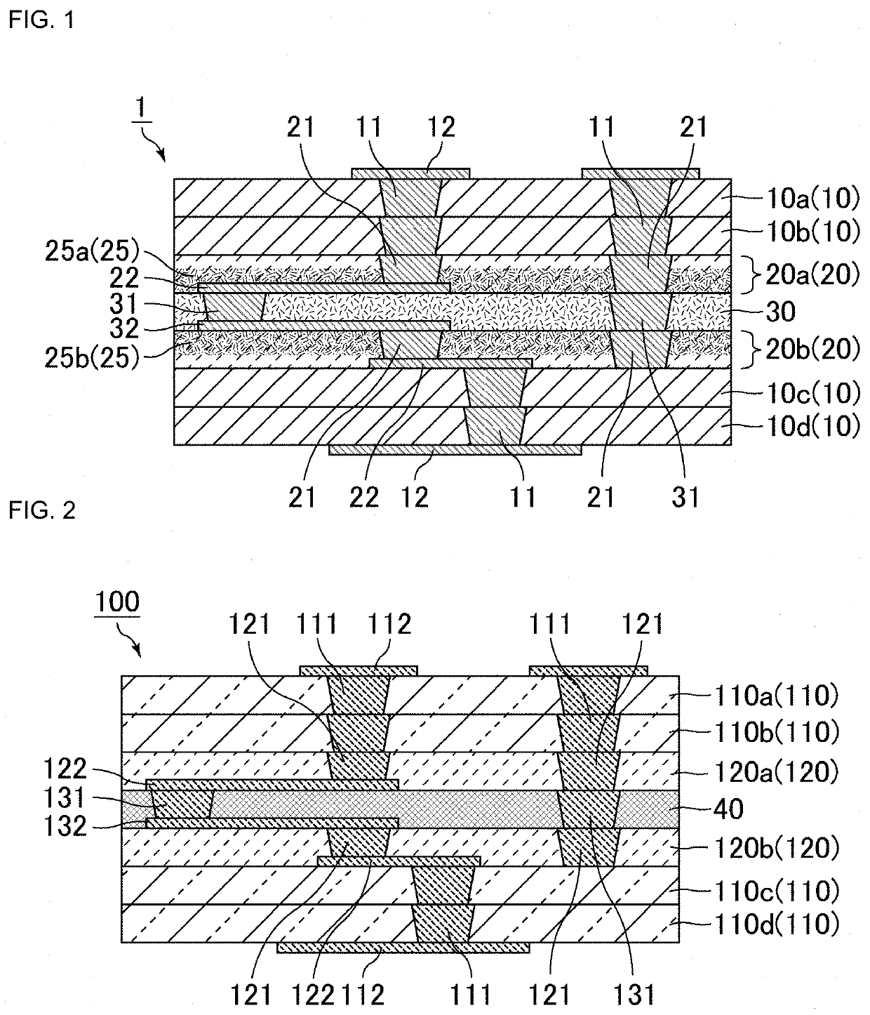
[0035]FIG. 1 is a schematic sectional view showing an example of the multilayer substrate according to the present invention. The multilayer substrate 1 shown in FIG. 1 includes first ceramic layers 10 (10a, 10b, 10c, and 10d) that are dense bodies, second ceramic layers 20 (20a and 20b) that have open pores, and a resin layer 30. The second ceramic layers 20 are adjacent to the resin layer 30, and a material for forming the resin layer 30 diffuses into the second ceramic layers 20 (regions indicated by references 25a and 25b in FIG. 1).
[0036]The first ceramic layers 10 are provided with metal conductors 11 and metal wiring lines 12, the second ceramic layers 20 are provided with metal conductors 21 and metal wiring lines 22, and the resin layer 30 is provided with metal conductors 31 and a metal wiring line 32.
[0037]The first ceramic layer 10 is a ceramic layer that is a dense body. Here, “dense body” refers to a first ceramic layer with substantially no pores. Preferably, the firs...
second embodiment
[0106]In the multilayer substrate according to the present embodiment, the location of the resin layer is any one outermost layer or both outermost layers of the multilayer substrate. The resin layer located as the outermost layer is adjacent to the second ceramic layer. Other configurations may be the same as in the multilayer substrate according to the first embodiment.
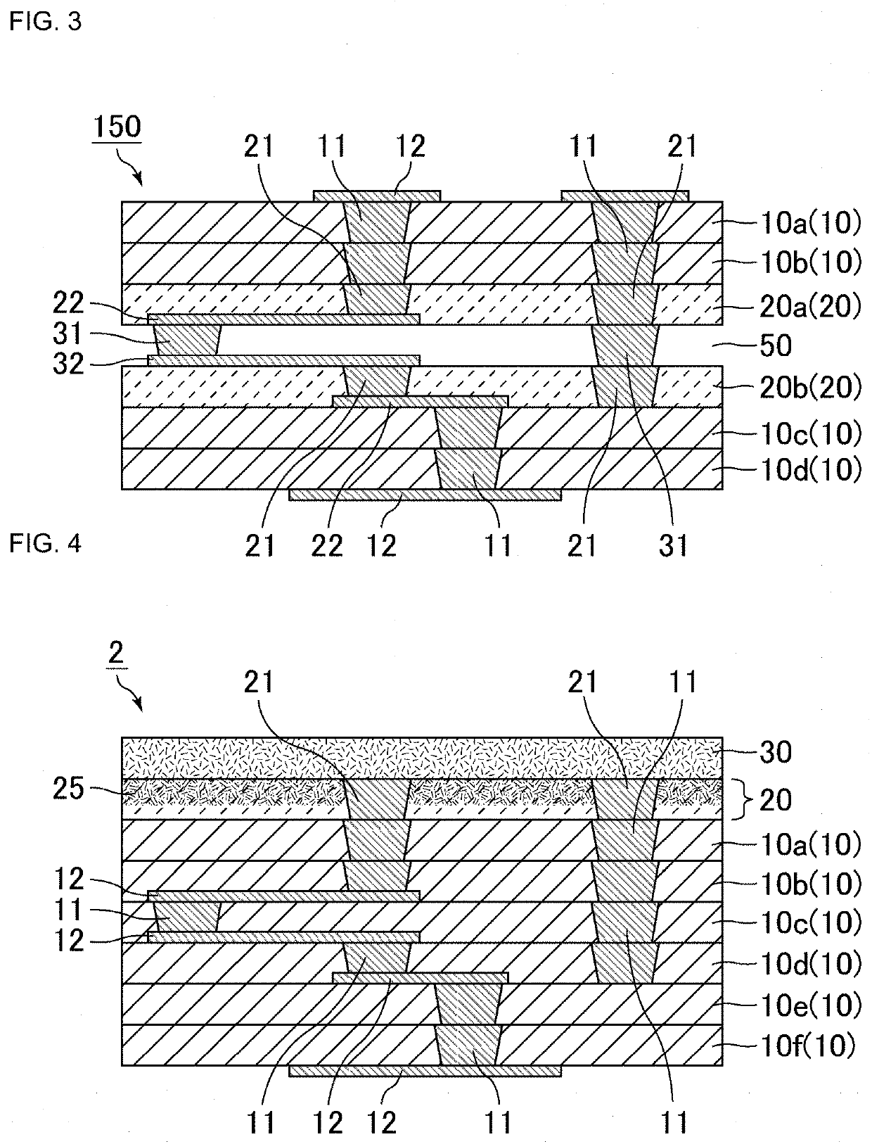
[0107]FIG. 4 is a schematic sectional view showing another example of the multilayer substrate according to the present invention. The multilayer substrate 2 includes first ceramic layers 10 (10a, 10b, 10c, 10d, 10e, and 10f) that are dense bodies, a second ceramic layer 20 having open pores, and a resin layer 30. The second ceramic layer 20 is adjacent to the resin layer 30, and a material for forming the resin layer 30 diffuses into the second ceramic layer 20 (region indicated by reference 25 in FIG. 4). In the multilayer substrate 2, the resin layer 30 is disposed as the outermost layer of the multilayer substra...
example 1
[0115]A powder containing SiO2, Al2O3, and BaCO3 serving as a ceramic powder was subjected to wet mixing and pulverization, and drying was performed so as to obtain a mixture. The resulting mixture was heat-treated so as to obtain a raw material powder for forming the first ceramic green sheet. An organic binder, a dispersing agent, and a plasticizer were added, and mixing and pulverization were performed so as to produce a slurry. The resulting slurry was formed into the shape of a sheet on a base material film by a doctor blade method and dried so as to obtain the first ceramic green sheets while adjusting the thickness such that the thickness after firing became a predetermined thickness.
[0116]Via holes were formed in the first ceramic green sheets by using a laser, and the via holes were filled with a metal conductor paste. In addition, wiring lines were formed by screen printing using the metal conductor paste. Cu serving as a metal material and the above-described ceramic powd...
PUM
| Property | Measurement | Unit |
|---|---|---|
| depth | aaaaa | aaaaa |
| porosity | aaaaa | aaaaa |
| porosity | aaaaa | aaaaa |
Abstract
Description
Claims
Application Information