Semiconductor device and manufacturing method therefor

a manufacturing method and semiconductor technology, applied in the direction of semiconductor devices, electrical appliances, basic electric elements, etc., can solve the problems of shrinking the feature size between integrated circuit transistors, increasing processing speed and power consumption, and significantly reducing the size of semiconductors, so as to reduce the risk of leakage or breakdown

Active Publication Date: 2020-01-02
SHANGHAI HUALI MICROELECTRONICS CORP
View PDF1 Cites 7 Cited by
  • Summary
  • Abstract
  • Description
  • Claims
  • Application Information

AI Technical Summary

Benefits of technology

[0018]According to the semiconductor device and the manufacturing method therefor provided in the present disclosure, it is possible to form self-aligned through-holes by means of a reverse through-hole process in a case of a reduced node size, so that the through-hole continues to be of the shape of a control gate, and compared with the prior art, the shape of the through-hole is more straight, and the defect of the through-hole OVL offset existing in the prior art is avoided, which effectively reduces the risk of leakage or breakdown from the drain to the control gate, and the performance of electrical characteristics of the semiconductor device is more excellent.

Problems solved by technology

Over 50 years, the size of semiconductors have been significantly reduced, which translates into an increasing processing speed and decreasing power consumption.
This means that the feature size between integrated circuit transistors is shrinking.
For an ETOX-structure non-volatile memory, in order to meet the high-density and high-performance market demands, a node target has gradually moved to less than 50 nm, an AA pitch is gradually reduced to less than 120 nm, and a control gate line width Line is less than 120 nm, however, if the size of a drain between floating gates is required to be small, it will be restricted by the difficulty of the drain through-hole process, and the through-hole OVL and the through-hole shape are both great challenges, which cannot be met by using conventional techniques.

Method used


Image

  • Semiconductor device and manufacturing method therefor
  • Semiconductor device and manufacturing method therefor
  • Semiconductor device and manufacturing method therefor

Examples


Embodiment Construction

[0051]The present disclosure is described below in detail in conjunction with the accompanying drawings and particular embodiments. It is noted that the embodiments described in conjunction with the accompanying drawings and particular embodiments are merely exemplary, and should not be construed as any limitation on the scope of protection of the present disclosure.

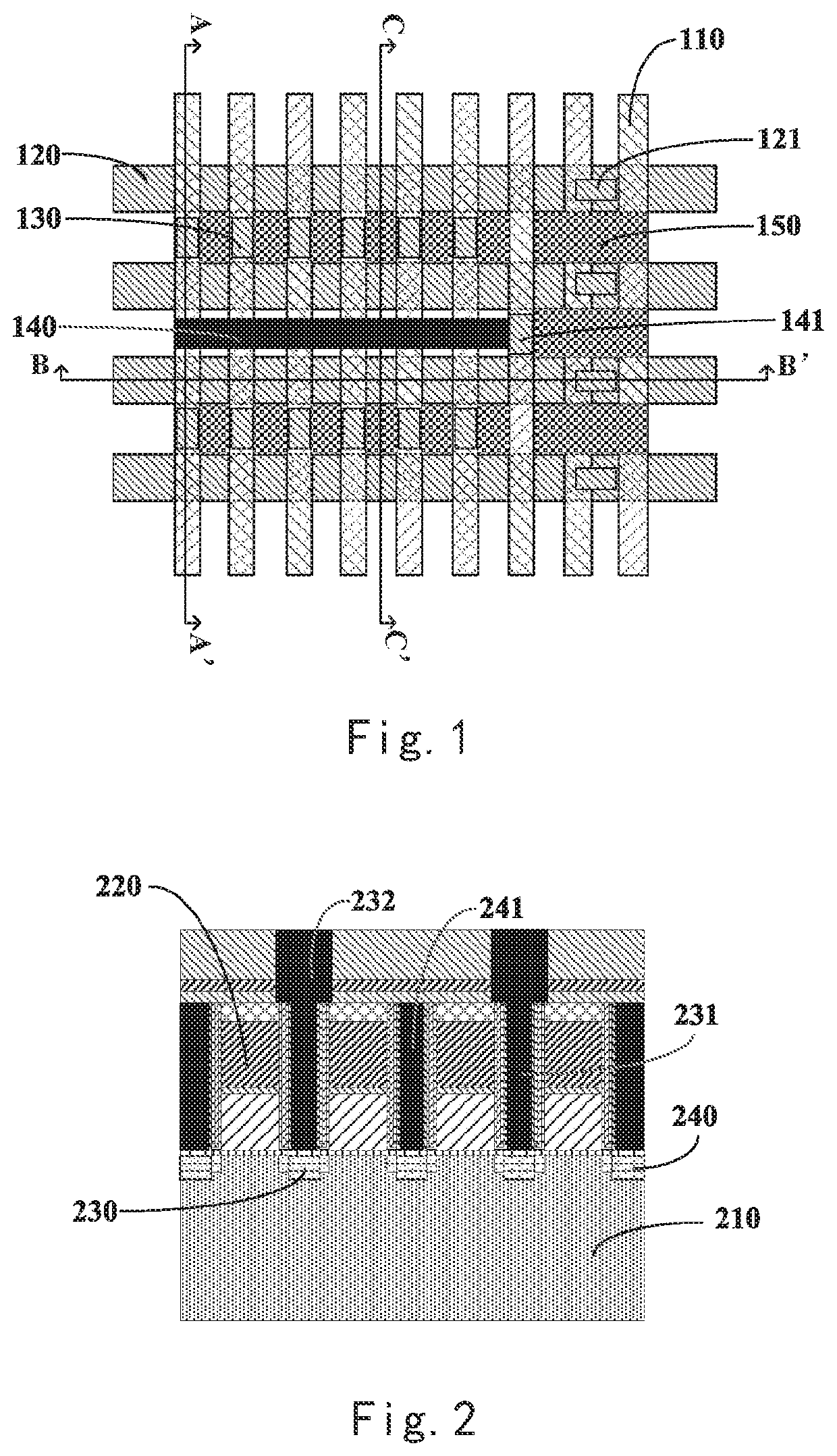
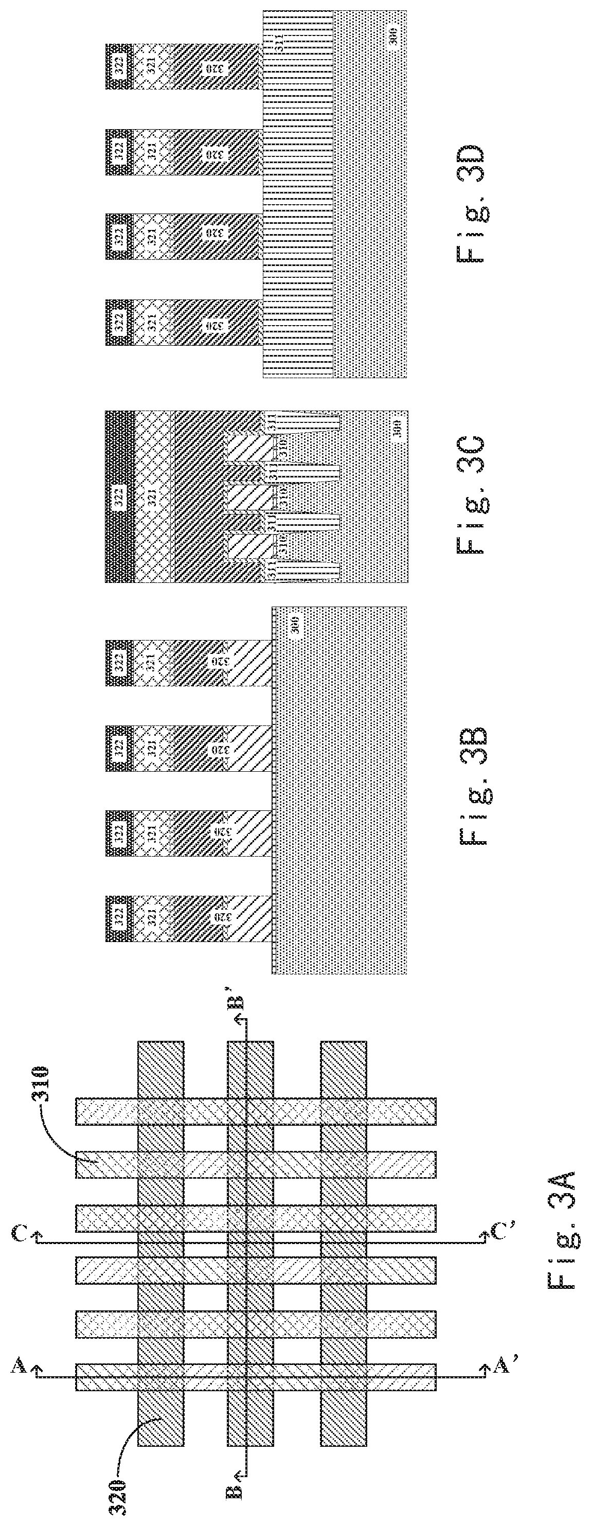
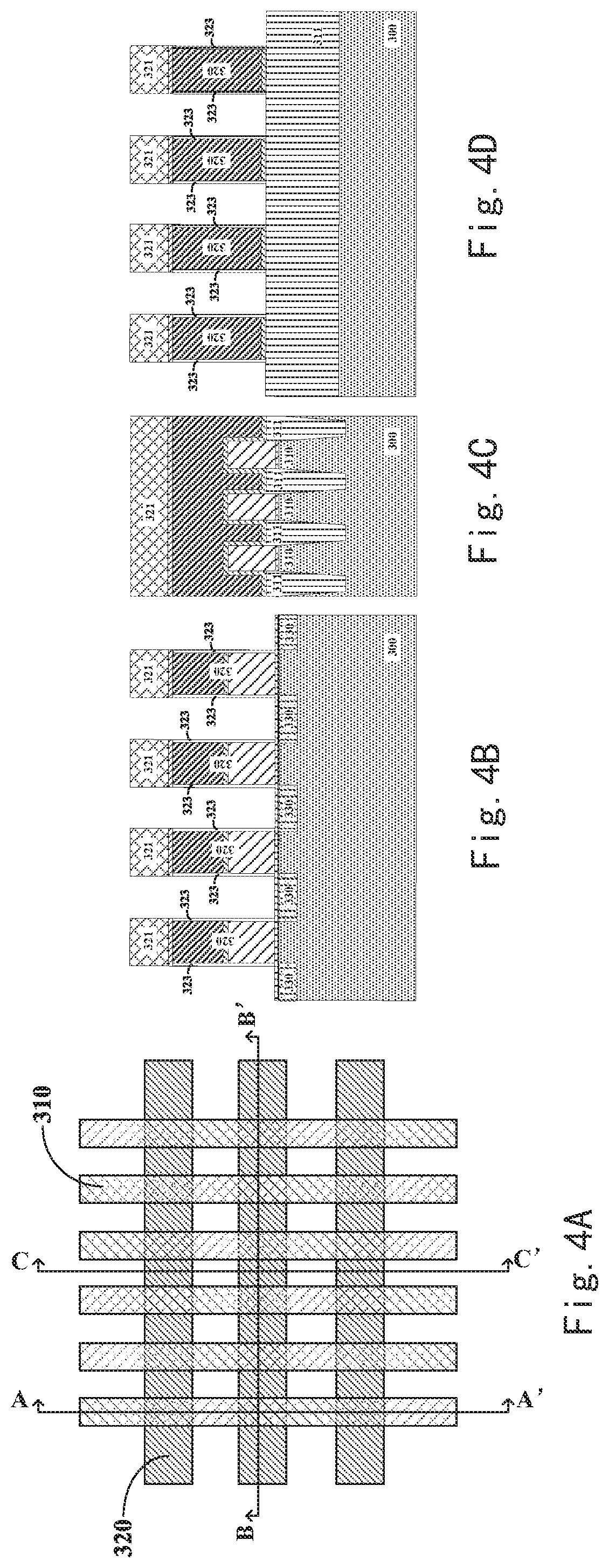
[0052]The present disclosure provides a manufacturing method for a semiconductor device. More specifically, an embodiment of the present disclosure provides a manufacturing method for a semiconductor device, and the manufacturing method comprises forming through-holes between semiconductor memories by forming a sacrificial layer between gates, by removing portions of the sacrificial layer to form isolation strips, and then by removing the sacrificial layer. By means of the reverse through-hole process, the through-hole continues to be of the shape of the gate, the shape is more straight, and there is no longitudinal OVL ...


PUM

PropertyMeasurementUnit
sizeaaaaaaaaaa
feature sizeaaaaaaaaaa

Abstract

The present disclosure provides a semiconductor device and a manufacturing method therefor. The manufacturing method for a semiconductor device is provided for forming through-holes in a semiconductor device, comprising: forming a plurality of shallow trench isolations in portions of a substrate corresponding to memory cell regions; forming a plurality of gates on surfaces of the portions of the substrate; forming spacers on side walls at both sides of the gates extending in the first direction; depositing a sacrificial layer on the memory cell region; removing portions of the sacrificial layer corresponding to the shallow trench isolations at memory cell drain, and depositing an isolation dielectric on the shallow trench isolations at the memory cell drain to form isolation strips; and removing the remaining sacrificial layer to form bottom through-holes in spaces formed after removing the remaining sacrificial layer.

Description

CROSS-REFERENCES TO RELATED APPLICATIONS[0001]The present application claims priority to Chinese Patent Application No. 201810714188.4, filed on Jun. 29, 2018, entitled “SEMICONDUCTOR DEVICE AND MANUFACTURING METHOD THEREFOR”, which is incorporated by reference herein for all purposes.FIELD[0002]The present disclosure relates to a manufacturing method for a semiconductor device and, in particular to a manufacturing method for a non-volatile memory.BACKGROUND OF THE DISCLOSURE[0003]Since the disclosure of integrated circuits by Dr. Jack Kilby of Texas Instruments in early years, scientists and engineers have made numerous disclosures and improvements in semiconductor devices and processes. Over 50 years, the size of semiconductors have been significantly reduced, which translates into an increasing processing speed and decreasing power consumption. To date, the development of semiconductors has largely followed Moore's Law, which roughly states that the number of transistors in dense...

Claims


Application Information

Patent Timeline
Patent Type & Authority Applications(United States)
IPC IPC(8): H01L27/11573H01L27/11565H01L21/762H01L21/768H01L21/311
CPCH01L27/11573H01L21/31116H01L21/76224H01L21/76837H01L27/11565H10B41/30H10B41/42H10B43/40H10B43/10
Inventor ZHANG, JINSHUANGCHEN, HAOYUWANG, QIWEIJI, FENG
Owner SHANGHAI HUALI MICROELECTRONICS CORP
Why Eureka
Try Eureka