Light emitting element for pixel and LED display module

a technology of led display module and light emitting element, which is applied in the direction of basic electric elements, electrical apparatus, and semiconductor devices, can solve the problems of difficult application, difficulty in achieving high resolution display modules, and limitation of miniaturizing led display modules

Active Publication Date: 2020-01-09
LUMENS
View PDF5 Cites 10 Cited by
  • Summary
  • Abstract
  • Description
  • Claims
  • Application Information

AI Technical Summary

Benefits of technology

[0042]According to the present disclosure, the micrometer-sized vertical LED chips are bonded to a support substrate formed with connection parts through bump balls and the connection parts are connected to wirings of the mount substrate through solders, avoiding the occurrence of remelting during manufacture. Since deposition points for connecting micrometer-sized wires on the upper surfaces

Problems solved by technology

However, this technology is difficult to apply to the fabrication of small-sized display modules and has difficulty in achieving high resolution of display modules.
Thus, there remai

Method used


Image

  • Light emitting element for pixel and LED display module
  • Light emitting element for pixel and LED display module
  • Light emitting element for pixel and LED display module

Examples


embodiments a

Embodiment A-1

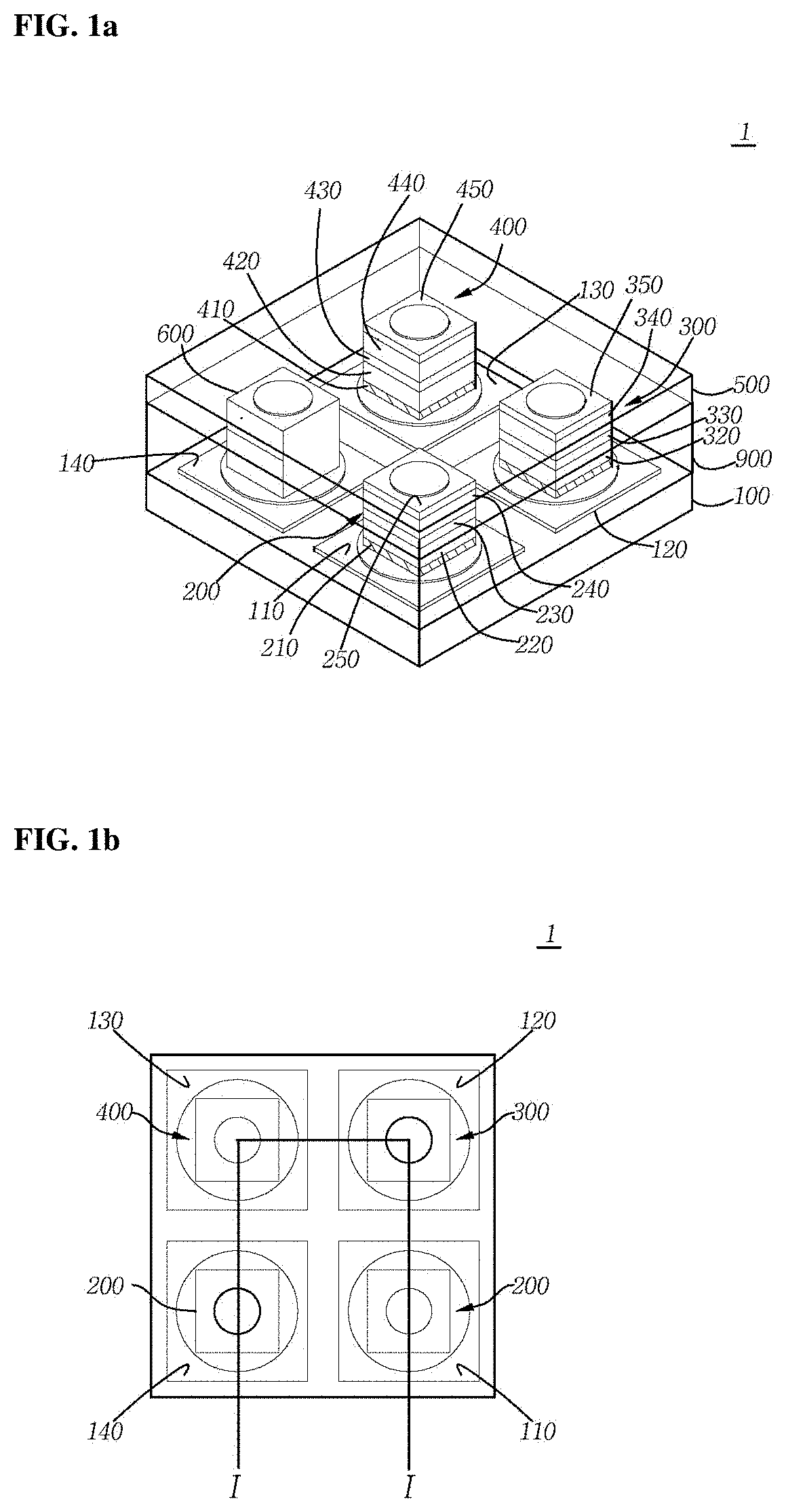
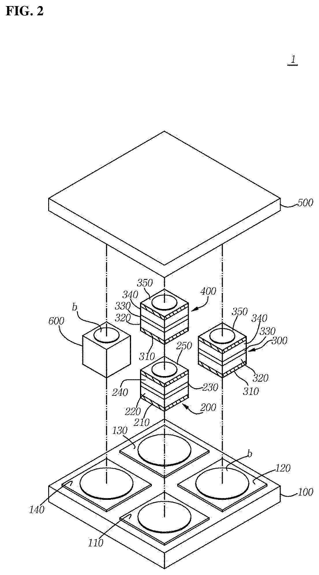
[0072]Referring to FIGS. 1a, 1b, 2, and 3, a light emitting element 1 for a pixel according to Embodiment A-1 includes a mount substrate 100, a first vertical LED chip 200, a second vertical LED chip 300, a third vertical LED chip 400, and a light-transmitting conductive plate 500.

[0073]The mount substrate 100 is substantially quadrangular in shape. A first electrode pad 110, a second electrode pad 120, a third electrode pad 130, and a fourth electrode pad 140 are disposed on the upper surface of the mount substrate 100. The electrode pads are arranged in a quadrangular array. The mount substrate 100 may be a printed circuit board (PCB).

[0074]The light-transmitting conductive plate 500 is spaced apart from the upper surface of the mount substrate 100. The light-transmitting conductive plate 500 can be made by coating indium tin oxide (ITO) on a light-transmitting plate such as a glass plate. ITO may be coated over the entire area of one surface of the light-transmittin...

embodiment a-2

[0104]In this embodiment, resistors may be further arranged under the light-transmitting conductive plate 500 to achieve white emission, as illustrated in FIG. 12. FIG. 12 illustrates a light emitting element for a pixel according to Embodiment A-2. As illustrated in (a) of FIG. 12, resistors 710, 720, and 730 are arranged between the top portion of the first vertical LED chip 200 and the conductor 600, between the top portion of the second vertical LED chip 300 and the conductor 600, and between the top portion of the third vertical LED chip 400 and the conductor 600 under the light-transmitting conductive plate 500 (see FIG. 1a or 2). (b) of FIG. 12 is an equivalent circuit diagram of the structure illustrated in (a). This arrangement of the resistors 710, 720, and 730 can achieve white emission. Furthermore, an integrated circuit (IC) may be further arranged under the light-transmitting conductive plate 500, achieving full-color display.

embodiment a-3

[0105]Referring to FIGS. 13 to 16, an LED display module 1000 according to Embodiment A-3 includes a rectangular mount substrate 100, a light-transmitting conductive plate 500 having almost the same shape and area as the mount substrate 100 and spaced apart from the mount substrate 100, and a plurality of pixel units 2 arrayed in a matrix between the mount substrate 100 and the light-transmitting conductive plate 500. Each of the plurality of pixel units 2 includes a first vertical LED chip 200, a second vertical LED chip 300, a third vertical LED chip 400, and a conductor 600.

[0106]The mount substrate 100 includes a plurality of pad groups G arrayed in a matrix and corresponding to the plurality of pixel units 2 on the upper surface thereof. Each of the plurality of pad groups G includes a first electrode pad 110, a second electrode pad 120, a third electrode pad 130, and a fourth electrode pad 140 disposed in a substantially rectangular array on the upper surface of the mount subs...


PUM


Abstract

A light emitting element is disclosed. The light emitting element includes: a mount substrate on which a first electrode pad, a second electrode pad, a third electrode pad, and a fourth electrode pad are disposed; a first vertical LED chip mounted on the mount substrate such that the bottom portion of the first vertical LED chip is connected to the first electrode pad; a second vertical LED chip mounted on the mount substrate such that the bottom portion of the second vertical LED chip is connected to the second electrode pad; a third vertical LED chip mounted on the mount substrate such that the bottom portion of the third vertical LED chip is connected to the third electrode pad; a light-transmitting conductive plate electrically connected to the top portions of the first vertical LED chip, the second vertical LED chip, and the third vertical LED chip; and a conductor connecting the light-transmitting conductive plate to the fourth electrode pad. Individual driving powers are applied to the first vertical LED chip, the second vertical LED chip, and the third vertical LED chip through the first electrode pad, the second electrode pad, and the third electrode pad, respectively, or through the fourth electrode pad.

Description

BACKGROUND OF THE INVENTION1. Field of the Invention[0001]The present invention relates to a light emitting element for a pixel in which small-sized R, G, and B vertical LED chips are arranged at small intervals in a small area, thus being suitable for use as a display pixel, and an LED display module in which a plurality of pixel units, each including first, second, third, and fourth vertical LED chips, are arrayed between a mount substrate and a light-transmitting plate and are individually driven by light-transmitting electrode patterns formed on the light-transmitting plate and first, second, third, and fourth electrode pads formed on the substrate.2. Description of the Related Art[0002]In typical full-color LED display modules, pixels consist of red, green, and blue LEDs. LED display modules including pixels consisting of red, green, blue, and white LEDs have recently been proposed.[0003]Package-on-module and chip-on-module technologies are employed to achieve RGB emission for ...

Claims


Application Information

Patent Timeline
IPC IPC(8): H01L25/075H01L25/16H01L33/62H01L33/00
CPCH01L25/0753H01L33/0079H01L33/62H01L25/167H01L33/0093
Inventor YOO, TAEKYUNGOH, SEUNGHYUNJO, SUNGSIKKIM, MINPYOSHIN, JIYUKIM, DAEWON
Owner LUMENS
Why Eureka
Try Eureka