
Semiconductor package

Active Publication Date: 2020-01-16
SAMSUNG ELECTRONICS CO LTD
View PDF2 Cites 3 Cited by
  • Summary
  • Abstract
  • Description
  • Claims
  • Application Information

AI Technical Summary

Benefits of technology

This patent describes a semiconductor package that includes a package substrate, flip chip, interposer, bonding wire, and mold layer. The mold layer has a signal hole and dummy hole, which helps to improve signal quality and reduce interference. The package can be stacked on top of another package to create a more complex semiconductor device. The technical effect of this invention is to improve the performance and reliability of semiconductor packages.

Problems solved by technology

Therefore, warpage in which the package is twisted in a specific direction may occur during the manufacturing process such as when a mold layer that encapsulates the components on the substrate is formed.
Such a warpage may significantly lower the reliability of the packages.

Method used


Image

  • Semiconductor package
  • Semiconductor package
  • Semiconductor package

Examples


Embodiment Construction

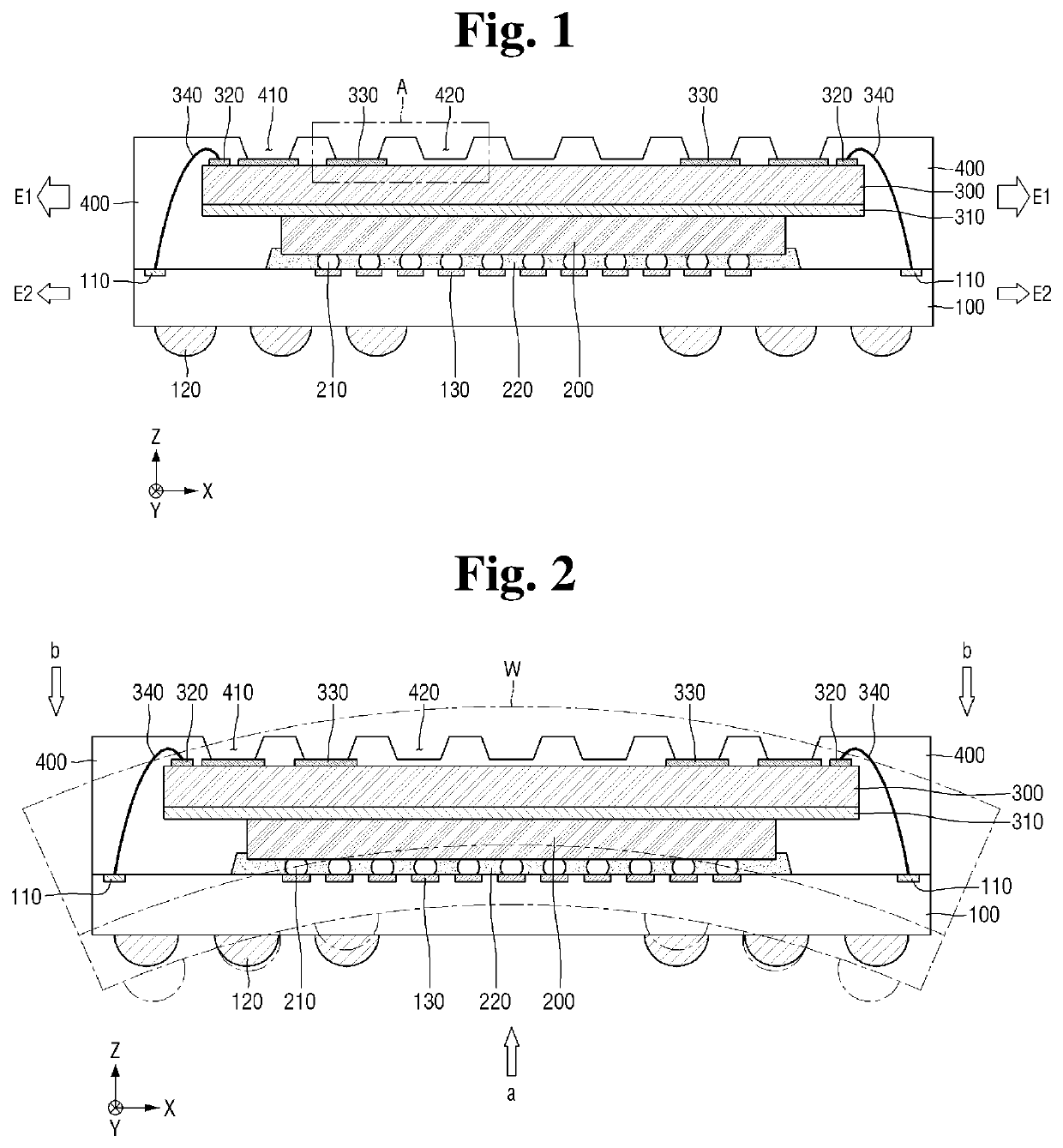
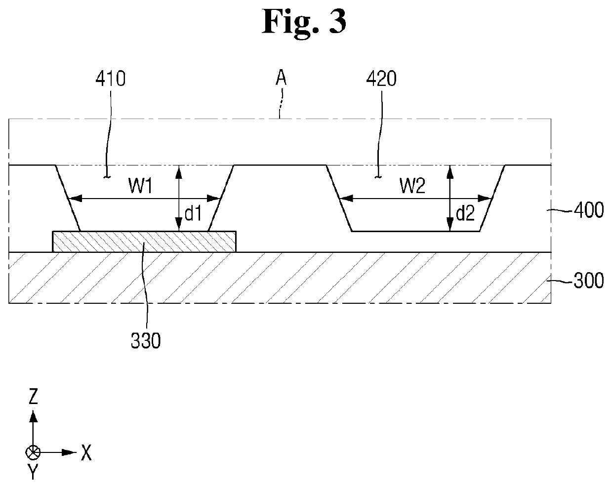
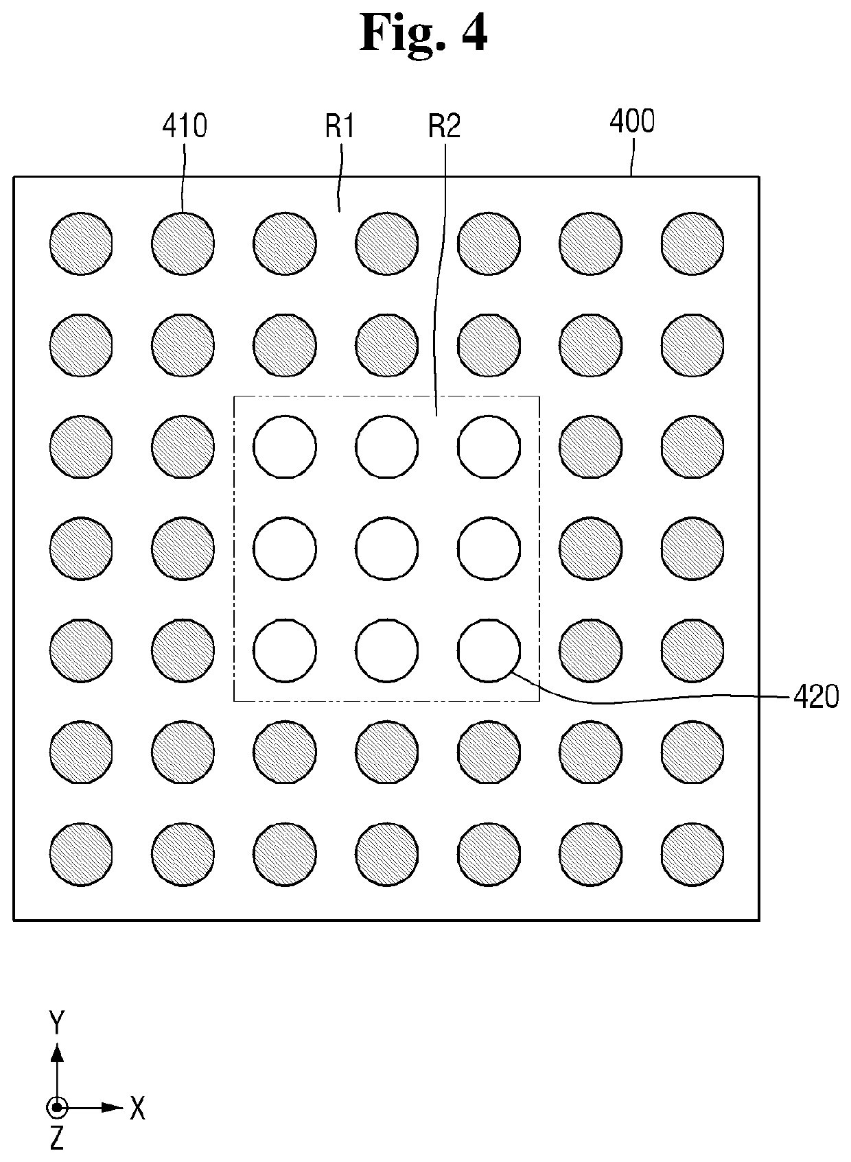
[0025]One example of a semiconductor package according to the inventive concept will now be described with reference to FIGS. 1 to 4.

[0026]In the figures, direction X is a first horizontal direction, and direction Y is a second horizontal direction intersecting the first direction X. The first direction X and the second direction Y may be perpendicular to each other. A third direction Z has a vertical component and intersects both the first direction X and the second direction Y. For example, the third direction Z may be a vertical direction, i.e., may be perpendicular to the first direction X and the second direction Y. In this case, the first direction X, the second direction Y, and the third direction Z may all orthogonal to each other.

[0027]Furthermore, in the description that follows, although the drawings show plural ones of like elements, the elements may be referred individually at times for ease of description. It will be understood that each description of a feature or asp...


PUM


Abstract

A semiconductor package includes a package substrate, a flip chip coupled to the package substrate, an interposer stacked on the flip chip and including a first terminal and a second terminal at an upper surface thereof, a bonding wire which connects the first terminal and the package substrate and a mold layer which covers the interposer, the flip chip and the bonding wire. The mold layer has a signal hole which exposes the second terminal, and at least one dummy hole spaced apart from the signal hole on an upper surface of the interposer.

Description

PRIORITY STATEMENT[0001]This application claims priority from Korean Patent Application No. 10-2018-0079925 filed on Jul. 10, 2018 in the Korean Intellectual Property Office, and all the benefits accruing therefrom under 35 U.S.C. 119, the contents of which in its entirety are herein incorporated by reference.BACKGROUND1. Field[0002]The inventive concept relates to a semiconductor package.2. Description of the Related Art[0003]The semiconductor industry is continuously attempting to miniaturize and reduce the thickness and weight of semiconductor products while maintaining a high degree of integration of the products. To these ends, various types of packages having a stack of components mounted on a substrate have been developed and their applications and use are gradually increasing.[0004]However, the stacked components of the package include various materials having different coefficient of thermal expansions. Therefore, warpage in which the package is twisted in a specific direct...

Claims


Application Information

Patent Timeline
IPC IPC(8): H01L23/49H01L23/31H01L23/00
CPCH01L23/49H01L24/08H01L23/3114H01L25/162H01L23/3128H01L23/315H01L23/481H01L24/14H01L2224/1413H01L2224/1411H01L25/0657H01L2225/0651H01L2225/06517H01L2225/06558H01L2225/06555H01L25/105H01L2225/1017H01L2225/1058H01L2224/73204H01L2224/73253H01L2924/19107H01L2924/15311H01L2924/1815H01L2924/3511H01L2224/0401H01L2224/0557H01L2224/16145H01L2224/16227H01L2224/32145H01L2224/32225H01L2224/17181H01L24/16H01L24/32H01L23/49816H01L23/49838H01L2225/1041H01L2225/06541H01L2924/00H01L2224/16225H01L24/97H01L24/45
Inventor KIM, YOUNG BAE
Owner SAMSUNG ELECTRONICS CO LTD
Learn More