
Flash memory controller, flash memory module and associated electronic device

Active Publication Date: 2020-01-23
SILICON MOTION INC (TW)
View PDF0 Cites 5 Cited by
  • Summary
  • Abstract
  • Description
  • Claims
  • Application Information

AI Technical Summary

Benefits of technology

The present invention aims to provide a method for accessing a memory device efficiently, even in a high-density storage arrangement. This method helps to obtain enough information for decoding operations and address the problems involved in accessing such devices.

Problems solved by technology

Improving access control of memories in these memory devices remains an issue to be solved in the art.
The MLC flash memory does have instability issues, however.
For example, as the triple level cell (TLC) flash memories have been applied to the memory devices, there are some problems such as an increased bit error rate, etc.
Although a traditional sensing scheme regarding reading data from the TLC flash memories has been proposed to try solving the problems, it does not work for the memory devices equipped with the quadruple level cell (QLC) flash memories.
More particularly, the traditional sensing scheme is not good for high-level per memory cell in the QLC flash memories.

Method used


Image

  • Flash memory controller, flash memory module and associated electronic device
  • Flash memory controller, flash memory module and associated electronic device
  • Flash memory controller, flash memory module and associated electronic device

Examples


first embodiment

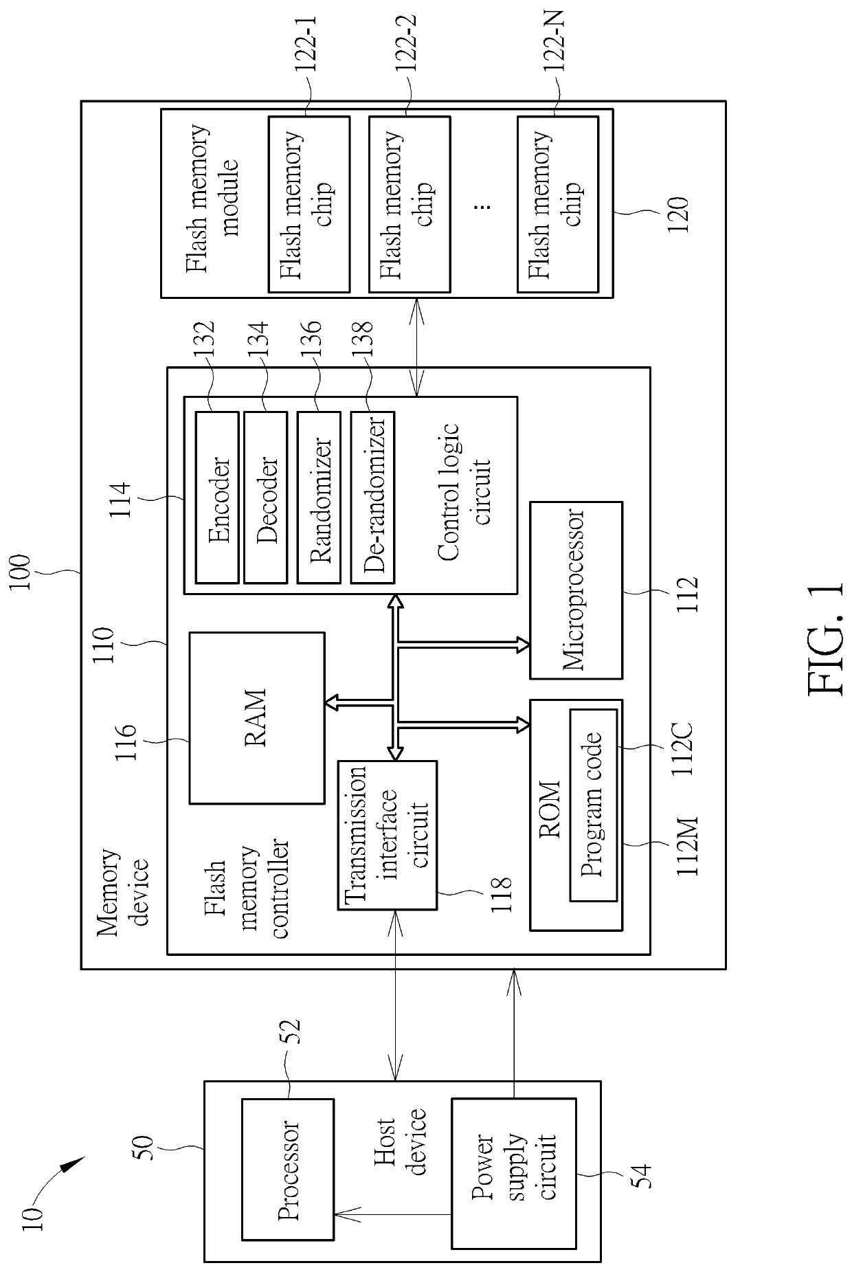
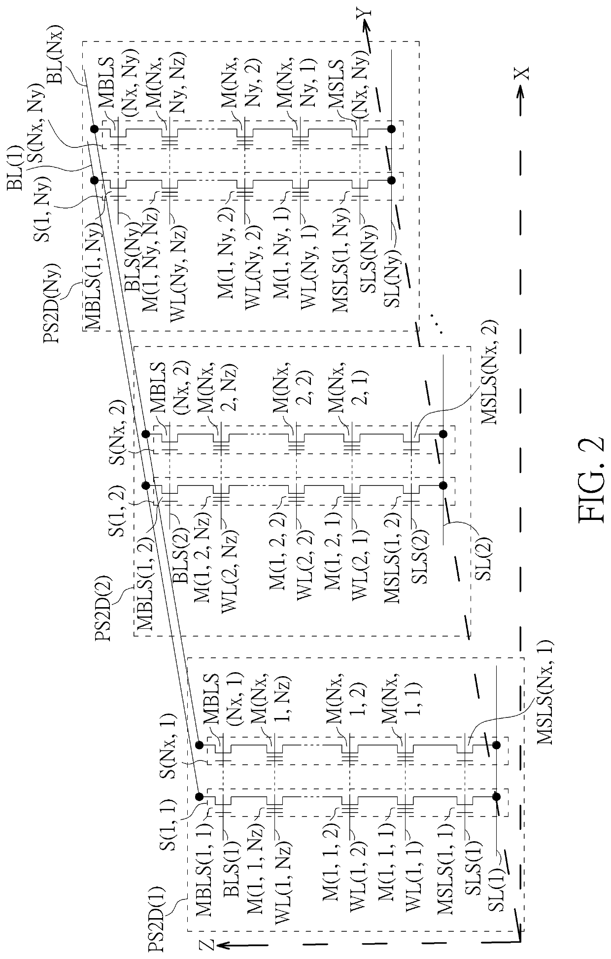
[0048]FIG. 7 is a diagram illustrating a sense amplifier 700 according to the present invention. In FIG. 7, the sense amplifier 700 comprises an operational amplifier 710, a voltage source 712, a control circuit 714, a counter 716 and a switch SW1. In this embodiment, the sense amplifier 700 is arranged to read the memory cell M(1, 1, Nz) corresponding to the bit line BL(1) and the word line WL(1, Nz) shown in FIG. 1. When the memory cell M(1, 1, Nz) is to be read, the control circuit 714 is configured to generate read voltage VR to the memory cell M(1, 1, Nz) shown in FIG. 1, the upper selector circuit MBLS(1, 1) and the other memory cells M(1, 1, 1)-M(1, 1, (Nz−1)) are controlled to be conductive.

[0049]Refer to FIG. 7 and FIG. 8 together, FIG. 8 is a timing diagram of some signals of the sense amplifier 700 according to one embodiment of the present invention. In the operations of the sense amplifier 700, initially the read voltage VR is equal to zero (i.e. the memory cell M(1, 1,...

second embodiment

[0073]FIG. 18 is a diagram illustrating a sense amplifier 1800 according to the present invention. In FIG. 18, the sense amplifier 1800 comprises an operational amplifier 1810, a voltage source 1812, a digital-to-analog converter 1814 and a switch SW1. In this embodiment, the sense amplifier 1800 is arranged to read the memory cell M(1, 1, Nz) corresponding to the bit line BL(1) and the word line WL(1, Nz) shown in FIG. 1. When the memory cell M(1, 1, Nz) is to be read, the DAC 1814 is configured to generate the read voltage VR to the memory cell M(1, 1, Nz) shown in FIG. 1, and the other memory cells M(1, 1, 1)-M(1, 1, (Nz−1)) are controlled to be conductive.

[0074]Refer to FIG. 18 and FIG. 19 together, FIG. 19 is a timing diagram of some signals of the sense amplifier 1800 according to one embodiment of the present invention. In the operations of the sense amplifier 1800, initially the DAC 1814 does not work and the read voltage VR is equal to zero (i.e. the memory cell M(1, 1, Nz)...


PUM


Abstract

The present invention provides a method for accessing a flash memory module, wherein the flash memory module comprises at least one flash memory chip, each flash memory chip comprises a plurality of blocks, each block comprises a plurality of pages, and the method includes the steps of: sending a read command to the flash memory module to ask for data on at least one memory unit; receiving multi-bit information of a plurality of memory cells of the at least one memory unit from the flash memory module; and analyzing the multi-bit information of the plurality of memory cells to obtain a threshold voltage distribution of the plurality of memory cells for determining a decoding process.

Description

CROSS REFERENCE TO RELATED APPLICATIONS[0001]This application claims the priority of U.S. Provisional Application No. 62 / 700,345, filed on Jul. 19, 2018, which is included herein by reference in its entirety.BACKGROUND OF THE INVENTION1. Field of the Invention[0002]The present invention relates to access control of flash memory, and more particularly, to a method for performing access management of a flash memory module and associated flash memory controller and electronic device.2. Description of the Prior Art[0003]Developments in memory technology have led to the wide application of portable or non-portable memory devices, such as memory cards which conform to the SD / MMC, CF, MS and XD specifications, respectively, solid state drives (SSDs), or embedded memory devices which conform to the Universal Flash Storage (UFS) and embedded Multi Media Card (eMMC) specifications, respectively. Improving access control of memories in these memory devices remains an issue to be solved in the ...

Claims


Application Information

Patent Timeline
IPC IPC(8): G06F3/06G11C11/56G11C16/04G11C16/10G11C16/26
CPCG11C16/26G06F3/0659G06F3/0604G11C16/10G11C16/0483G06F3/0679G11C2216/14G11C11/5628G11C11/5642G11C16/08G11C16/28G11C11/5621G06F3/064G06F3/0688H03M13/1105G06F3/0616
Inventor YANG, TSUNG-CHIEH
Owner SILICON MOTION INC (TW)
Learn More