Method of forming cavity in printed circuit board by using release film

a technology of printed circuit boards and release films, which is applied in the field of forming cavities in printed circuit boards, can solve the problems of reducing the yield of cavity formation, and increasing the defect rate, and achieves the effects of low manufacturing cost, mass production, and easy processing

Inactive Publication Date: 2020-01-23
TLB
View PDF0 Cites 0 Cited by
  • Summary
  • Abstract
  • Description
  • Claims
  • Application Information

AI Technical Summary

Benefits of technology

[0028]The method is advantageous in terms of easy processing, mass production, and low manufacturing cost for printed circuit boards.
[0029]Further, a cavity having an exactly same size as an actually required size can be designed for a printed circuit board, and it is possible to prevent an adhesive component from seeping out into a cavity from prepregs during formation of the cavity.
[0030]In addition, it is possible to prevent a poor connection between components attributable to collapsing of the prepregs.

Problems solved by technology

However, due to inevitable actual machining errors, the residue 122-2 of the copper clad 122 undesirably remains in the vicinity of the cavity 120.
This concern is a factor of remarkably reducing the cavity formation yield and increasing the defect rate.
In addition, there is a problem that the adhesive component seeps out from the adjacent prepreg 110 due to the pressure and heat applied during the laser drilling process.
However, even though a non-flow prepreg is used, a liquid component containing an adhesive component included in the prepreg seeps out during a cavity formation process.
Therefore, additional work is required to form the cavity having an actually required size.
This results in a decrease in the production yield.
Thus, a circuit portion formed on the outermost layer substrate 130 located on the prepreg having collapsed is likely to be disconnected from an electronic component connected thereto, resulting in that the defect rate increases.

Method used


Image

  • Method of forming cavity in printed circuit board by using release film
  • Method of forming cavity in printed circuit board by using release film
  • Method of forming cavity in printed circuit board by using release film

Examples


Embodiment Construction

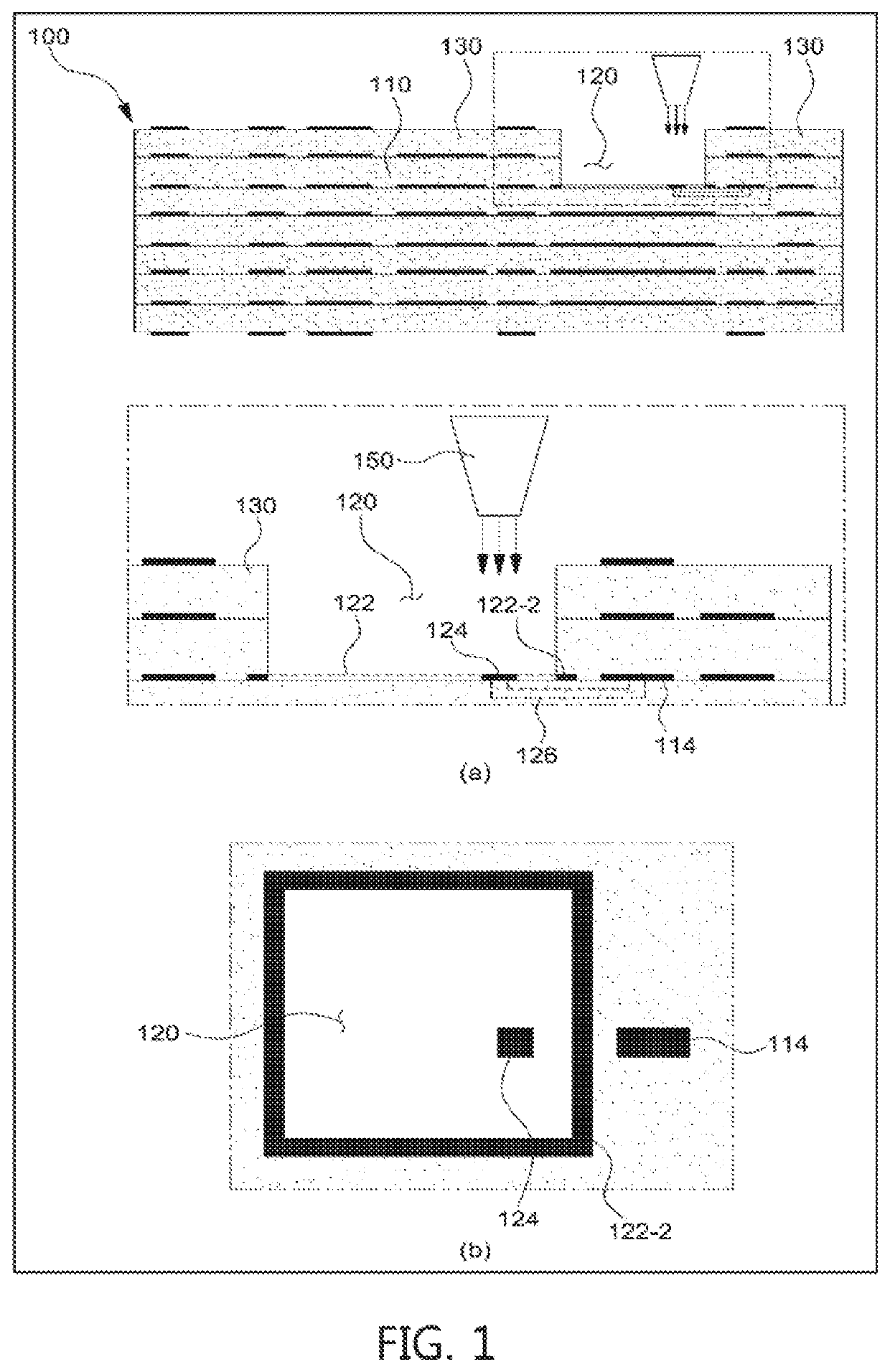
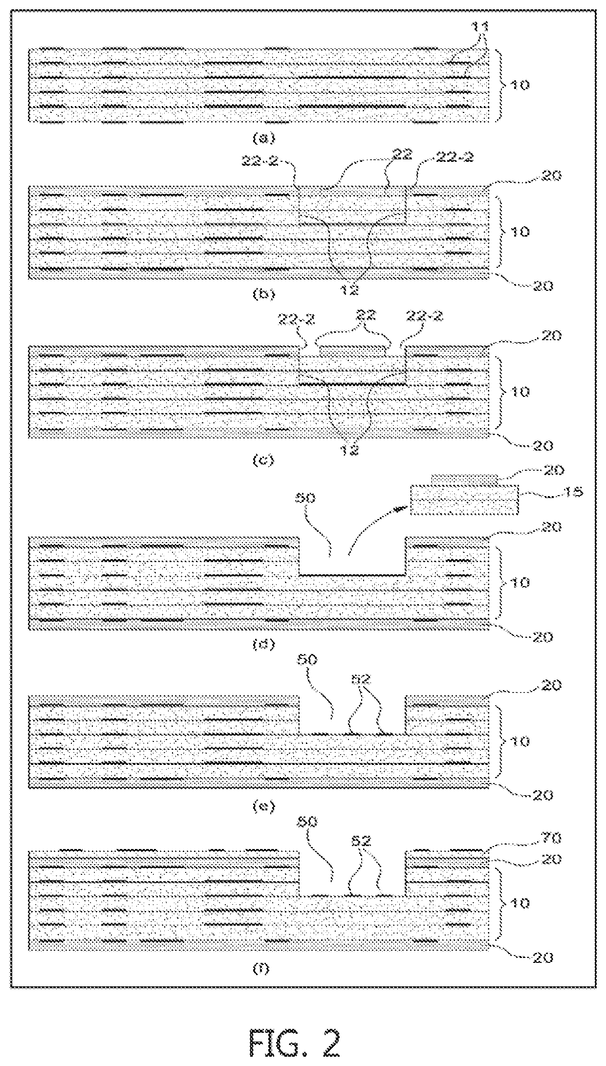
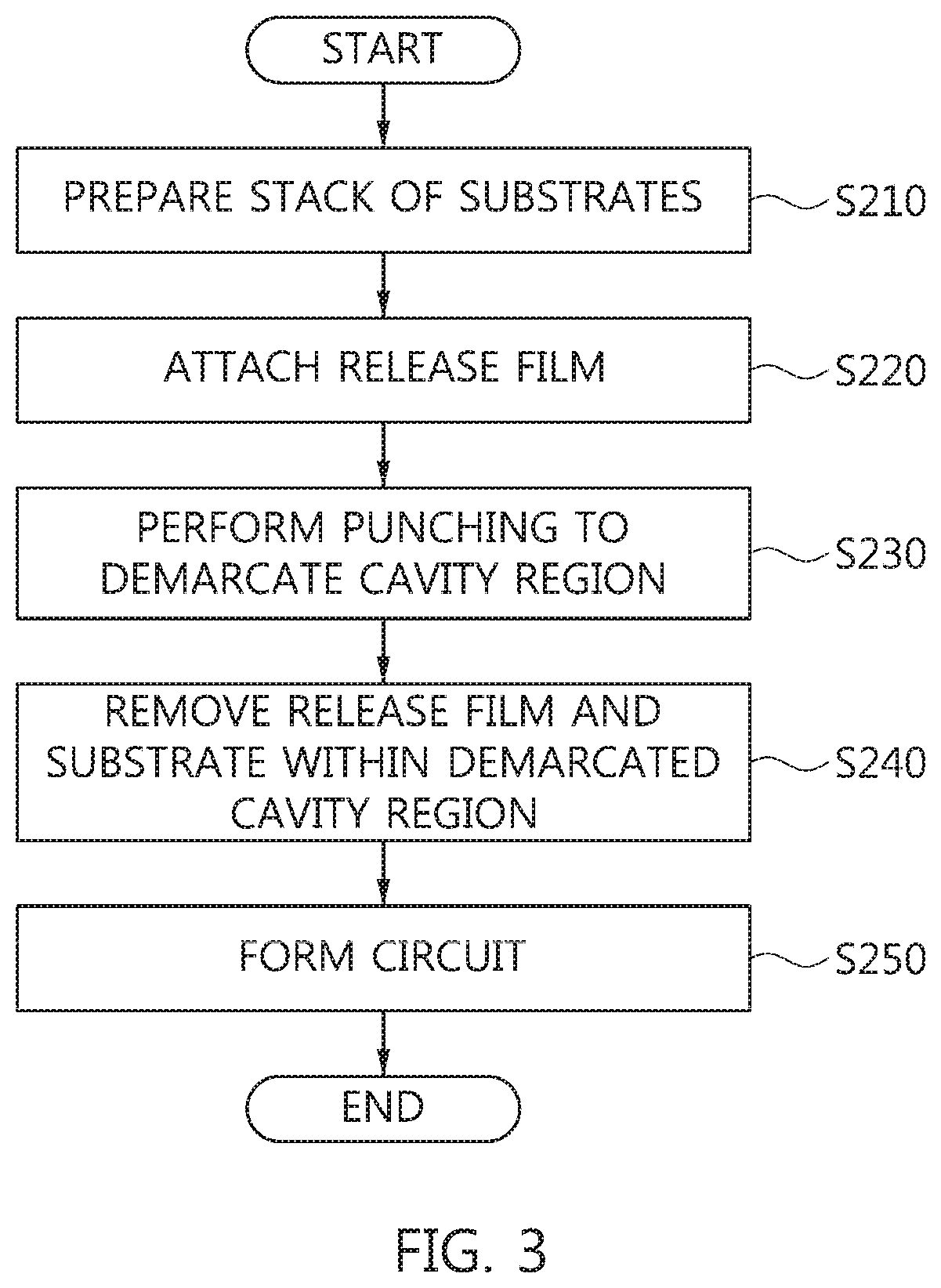
[0036]Hereinbelow, exemplary embodiments of the present invention will be described in detail with reference to the accompanying drawings.

[0037]Prior to giving the following detailed description of the present disclosure, it should be noted that terms used in the specification and the claims should not be construed as being limited to ordinary meanings or dictionary definitions but should be construed in a sense and concept consistent with the technical idea of the present disclosure, on the basis that the inventor can properly define the concept of a term to describe his or her invention in best way possible.

[0038]Meanwhile, the exemplary embodiments described in the specification and the configurations illustrated in the drawings are merely examples and do not exhaustively present the technical spirit of the present invention. Accordingly, it should be appreciated that there may be various equivalents and modifications that can replace the exemplary embodiments and the configurati...


PUM

PropertyMeasurementUnit
thicknessaaaaaaaaaa
thicknessaaaaaaaaaa
thicknessaaaaaaaaaa

Abstract

Disclosed is a cavity forming method for a printed circuit board. The method includes: stacking a plurality of substrates to form a stacked structure, each substrate including a prepreg and a copper clad circuit formed on a surface of the prepreg; attaching a release film to an outer surface of the stacked structure; demarcating a cavity region by forming a cutting line in the release film and the underlying prepreg; and removing the released film and the underlying prepreg inside the demarcated cavity region, thereby forming a cavity. The method is advantageous in terms of easy processing, mass production, and low manufacturing cost for printed circuit boards. Further, a cavity having an exactly same size as an actually required size can be designed for a printed circuit board, and it is possible to prevent an adhesive component from seeping out into a cavity from prepregs during formation of the cavity.

Description

CROSS REFERENCE TO RELATED APPLICATION[0001]The present application claims priority to Korean Patent Application No. 10-2018-0083615, filed Jul. 18, 2018, the entire contents of which is incorporated herein for all purposes by this reference.BACKGROUND OF THE INVENTIONField of the Invention[0002]The present invention relates to a method of forming a cavity in a printed circuit board. More particularly, the present invention relates to a method of forming a cavity in a printed circuit board, the method being easy to perform, being suitable for mass production of printed circuit boards, being capable of suppressing an adhesive component from seeping out from a prepreg during a cavity formation process, and being capable of allowing engineers to design the same size cavity as a cavity that is actually required.Description of the Related Art[0003]Recently, electronics-related technologies have been focused on development of multi-functional and high-speed electronic products. Responding...

Claims


Application Information

Patent Timeline
Patent Type & Authority Applications(United States)
IPC IPC(8): H05K3/46H05K1/03H05K3/02H05K3/04
CPCH05K3/022H05K1/0366H05K3/048H05K1/0373H05K3/4697H05K3/005H05K3/0044H05K3/06
Inventor KIM, BUM-SEOKPARK, DAE-SOO
Owner TLB
Why Eureka
Try Eureka