Light-emitting diode package structure and manufacturing method thereof

a technology of light-emitting diodes and package structures, applied in the direction of sustainable manufacturing/processing, final product manufacturing, printed circuit aspects, etc., can solve the problems of further affecting the yield, and achieve the effect of improving the alignment problem and increasing the yield of transfer

Active Publication Date: 2020-03-05
UNIMICRON TECH CORP
View PDF2 Cites 6 Cited by
  • Summary
  • Abstract
  • Description
  • Claims
  • Application Information

AI Technical Summary

Benefits of technology

[0004]The invention provides a light-emitting diode package structure capable of improving a poor alignment problem during transferring of light-emitting diodes and increasing yield of transferring.

Problems solved by technology

Nevertheless, the size of the die is extremely small, and a large amount of transferring is required, and thus, if the bonding process relies only on the precision of the alignment system of the machines, unfavorable alignment may be generated, so that the yield may further be affected.

Method used


Image

  • Light-emitting diode package structure and manufacturing method thereof
  • Light-emitting diode package structure and manufacturing method thereof
  • Light-emitting diode package structure and manufacturing method thereof

Examples


Embodiment Construction

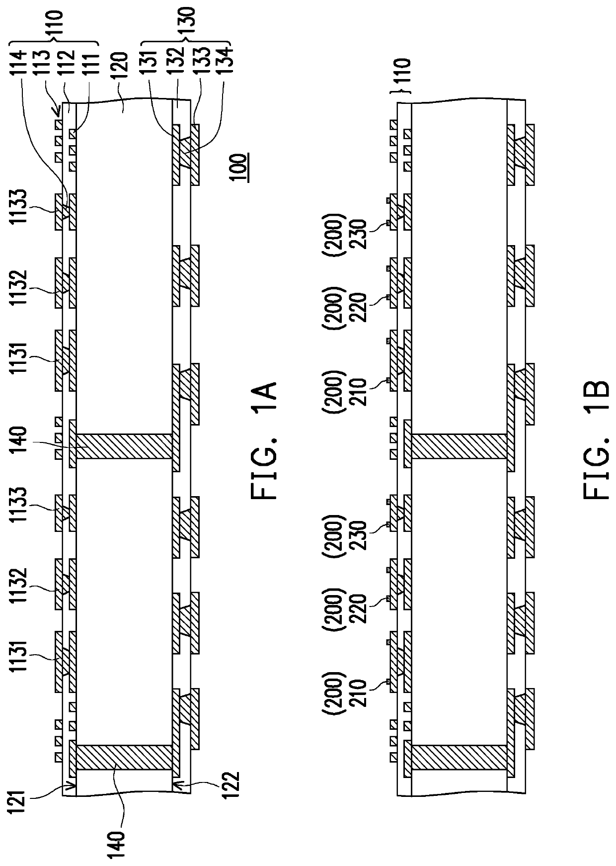
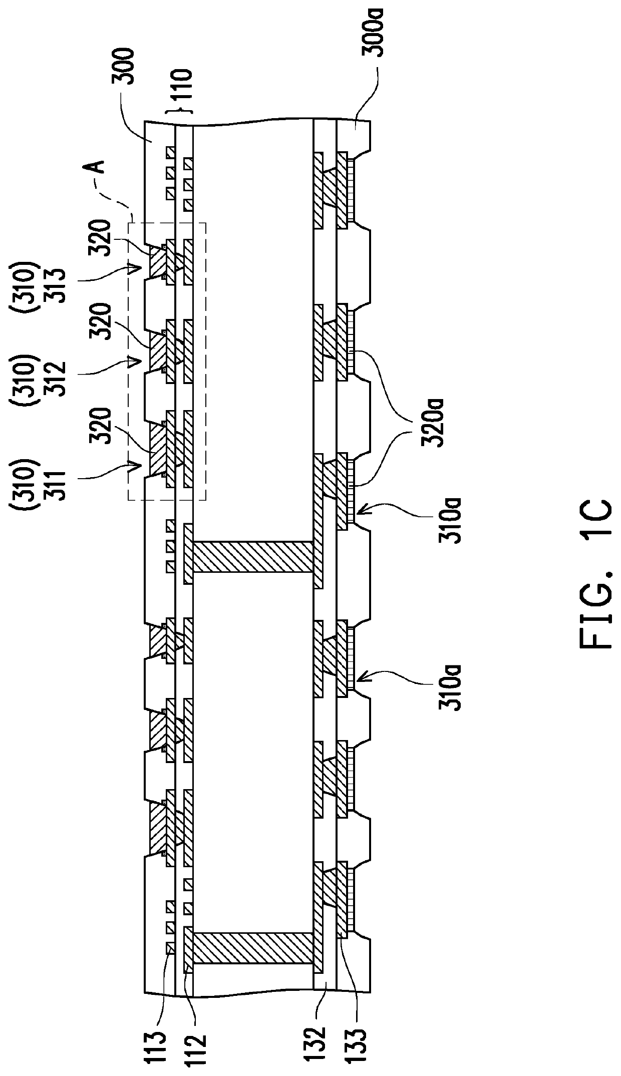
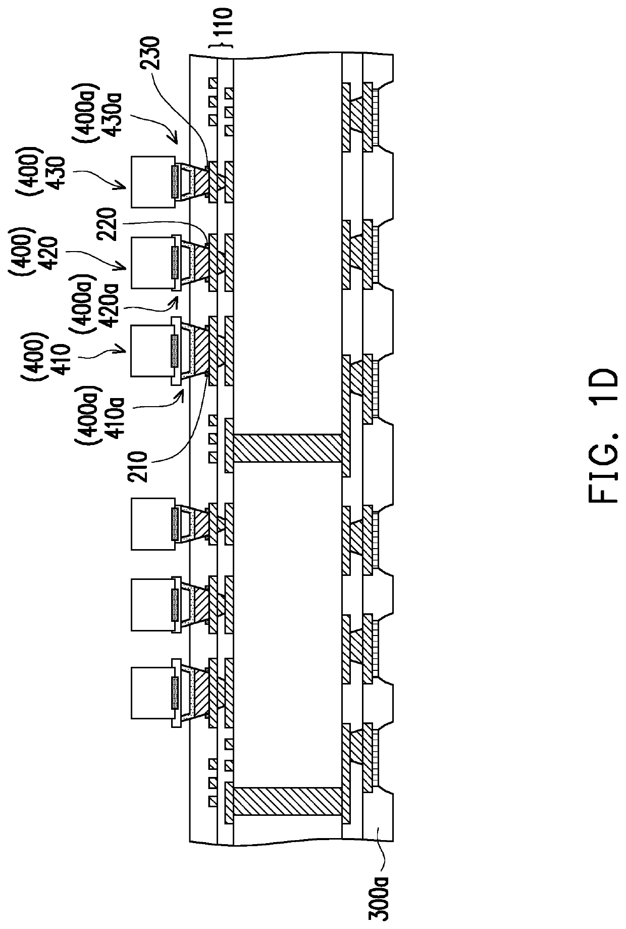
[0031]FIG. 1A to FIG. 1E are schematic cross-sectional views illustrating a manufacturing method of a light-emitting diode package structure according to an embodiment of the invention.

[0032]With reference to FIG. 1A, a carrier 100 is formed, and the carrier 100 at least includes a first build-up circuit 110. Specifically, in this embodiment, a substrate 120 is provided first, and the substrate 120 is drilled through a, for example, laser manner to form opening holes penetrating the substrate 120. Next, the opening holes are filled with a conductive material to form conductive through holes 140. The first build-up circuit 110 is formed on an upper surface 121 of the substrate 120, and a second build-up circuit 130 is formed on a lower surface 122 of the substrate 120. Herein, the first build-up circuit 110 includes a first conductive layer 111, a first dielectric layer 112, a second conductive layer 113, and a first conductive hole 114 penetrating the first dielectric layer 112. The...


PUM

PropertyMeasurementUnit
sizeaaaaaaaaaa
sizeaaaaaaaaaa
conductiveaaaaaaaaaa

Abstract

A light-emitting diode package structure includes a carrier, at least one self-assembled material layer, a first solder mask layer, and at least one light-emitting diode. The carrier includes a first build-up circuit. The self-assembled material layer is disposed on the first build-up circuit. The first solder mask layer is disposed on the first build-up circuit. The first solder mask layer has at least one opening to expose a portion of the self-assembled material layer. The light-emitting diode is disposed on the first build-up circuit. The light-emitting diode has a self-assembled pattern. The light-emitting diode is self-assembled into the opening of the first solder mask layer through a force between the self-assembled pattern and the self-assembled material layer. A manufacturing method of the light-emitting diode package structure is also provided.

Description

CROSS REFERENCE TO RELATED APPLICATION[0001]This application claims the priority benefit of Taiwan application serial no. 107130865, filed on Sep. 3, 2018. The entirety of the above-mentioned patent application is hereby incorporated by reference herein and made a part of specification.BACKGROUNDTechnical Field[0002]The invention relates to a light-emitting diode package structure and a manufacturing method thereof. More particularly, the invention relates to a light-emitting diode package structure featuring self-assembling and a manufacturing method thereof.Description of Related Art[0003]Currently, the non-solder mask define (NSMD) structure is used in the back plate structure of the mini light-emitting diodes (mini LEDs) or the micro light-emitting diodes (μLEDs) most of the time. In order to enhance fineness and resolution of screens, matrixes of high-density are required to be arranged for assembling, and a massive amount of transferring operation is also required. In the asse...

Claims


Application Information

Patent Timeline
Patent Type & Authority Applications(United States)
IPC IPC(8): H01L25/16H01L25/075H01L33/62H01L23/00
CPCH01L33/62H01L2224/2402H01L24/24H01L24/81H01L2933/0033H01L24/16H01L2224/24146H01L2224/24147H01L2224/81143H01L2933/0066H01L25/0753H01L2924/01026H01L2224/16141H01L25/167H01L2924/01028H01L2224/16227H01L2224/24227H01L2224/245H01L2224/24011H01L2924/01027H01L2924/181H01L2224/83902H01L2224/83143H01L2924/12041H01L2224/29111H01L2224/81411H01L2224/16237H01L2224/13111H01L2224/81005H01L2224/32237H01L2224/32227H01L24/13H01L24/29H01L24/32H01L24/83H01L23/5389H01L23/5384H05K2203/168H05K3/325H05K3/284H05K2201/10106H05K2203/104H05K1/111H05K2203/0186H05K2201/099Y02P70/50H01L2924/00012H01L2924/01047H01L2924/01029H01L2924/01004H01L2924/01051
Inventor LIN, WEI-TICHIEN, CHUN-HSIENCHEN, FU-YANG
Owner UNIMICRON TECH CORP
Why Eureka
Try Eureka