Thin film deposition method

a thin film and deposition method technology, applied in chemical vapor deposition coatings, coatings, electric discharge tubes, etc., can solve the problems of uniformity of thin film deposited on the pattern top directly exposed to plasma and thin film deposited on the trench wall and the bottom less exposed to plasma, so as to reduce the magnitude of bias and reduce the mobility of active species

Active Publication Date: 2020-03-12
ASM IP HLDG BV
View PDF0 Cites 211 Cited by
  • Summary
  • Abstract
  • Description
  • Claims
  • Application Information

AI Technical Summary

Benefits of technology

[0026]The thin film deposition method may further include, when supplying the at least one material, performing at least one of the following operations: increasing a density of a...

Problems solved by technology

However, when a thin film is deposited on a pattern structure (e.g., a pattern structure having a trench) on a substrate by using plasma, characteristics of a thin film ...

Method used


Image

  • Thin film deposition method
  • Thin film deposition method
  • Thin film deposition method

Examples


Embodiment Construction

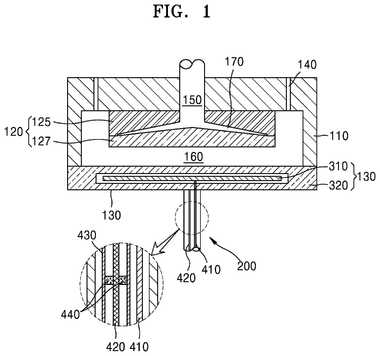
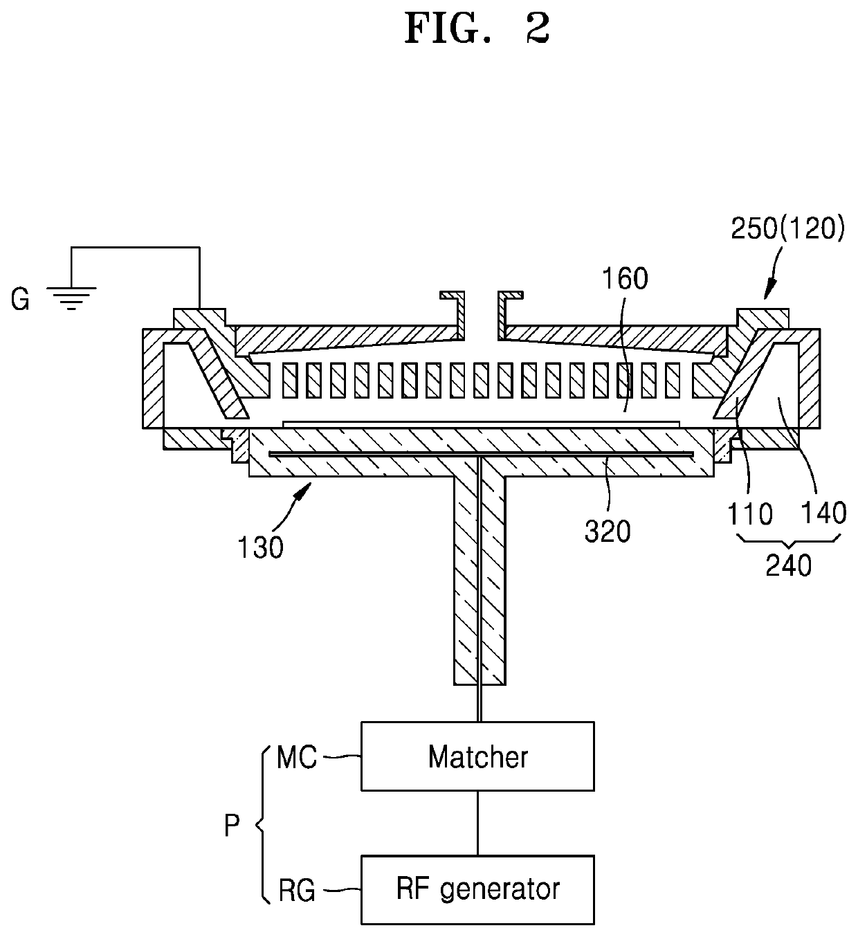
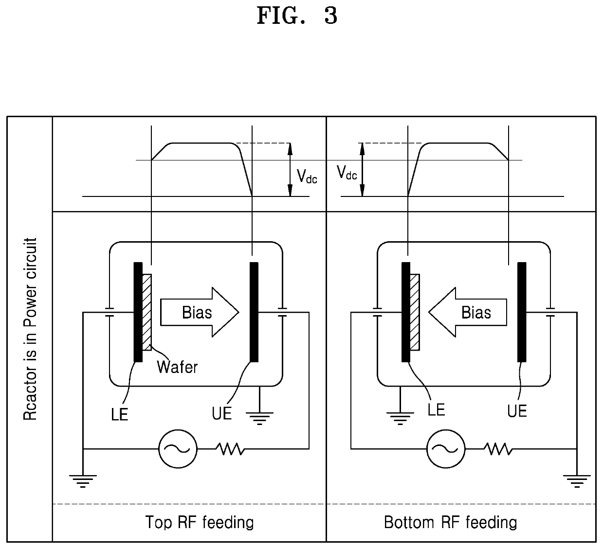
[0038]Reference will now be made in detail to embodiments, examples of which are illustrated in the accompanying drawings, wherein like reference numerals refer to like elements throughout. In this regard, the present embodiments may have different forms and should not be construed as being limited to the descriptions set forth herein. Accordingly, the embodiments are merely described below, by referring to the figures, to explain aspects of the present description. As used herein, the term “and / or” includes any and all combinations of one or more of the associated listed items. Expressions such as “at least one of,” when preceding a list of elements, modify the entire list of elements and do not modify the individual elements of the list.

[0039]Hereinafter, embodiments of the present disclosure will be described with reference to the accompanying drawings.

[0040]The embodiments of the present disclosure are provided to more fully describe the present disclosure to those of ordinary s...


PUM

PropertyMeasurementUnit
Timeaaaaaaaaaa
Timeaaaaaaaaaa
Timeaaaaaaaaaa

Abstract

A thin film deposition method with respect to a substrate including a pattern structure includes supplying RF power through a component disposed below a substrate, forming a potential on an exposed surface of the substrate exposed to a reaction space, moving the active species to the exposed surface in the reaction space using the potential, and forming a thin film including active species component on the exposed surface of the substrate.

Description

CROSS-REFERENCE TO RELATED APPLICATION[0001]This application claims the benefit of Korean Patent Application No. 10-2018-0108523, filed on Sep. 11, 2018, in the Korean Intellectual Property Office, the disclosure of which is incorporated herein in its entirety by reference.BACKGROUND1. Field[0002]One or more embodiments relate to a thin film deposition method, and more particularly, to a method of depositing a thin film on a pattern structure using plasma enhanced atomic layer deposition (PEALD).2. Description of the Related Art[0003]Plasma enhanced atomic layer deposition (PEALD) has the advantage of depositing a thin film, which may be deposited at a high temperature in existing thermal atomic layer deposition at a low temperature. This advantage may be achieved by sequentially introducing a reactive gas or a source gas at a time difference, activating and ionizing at least one of the gases by plasma.[0004]In a PEALD process, RF power is typically coupled to an upper electrode, e....

Claims


Application Information

Patent Timeline
IPC IPC(8): C23C16/455H01L21/02H01J37/32C23C16/458
CPCH01L21/02274H01J37/32724H01J37/32568C23C16/4586H01L21/0228H01J2237/3321H01J37/32174C23C16/45536C23C16/4581C23C16/45544C23C16/50C23C16/509C23C16/402H01L21/02164H01L21/02211H01L21/31111H01L21/68792H01L21/67248C23C16/505
Inventor UM, KICHULHAN, JEUNGHOONKIM, DOOHANHAN, YONGGYUYOO, TAEHEELIM, WANGYUKO, DONGHYUN
Owner ASM IP HLDG BV
Why Eureka
Try Eureka