
Phase modulators based on ambipolar field-effect transistors

a field-effect transistor and phase modulator technology, applied in the field of phase modulators, can solve the problems of inability to continuously variable phase modulation or broadband frequency use, non-flexible, non-transparent silicon that is not suitable for high-density, portable low-power consumption electronics, etc., to achieve the effect of improving the functionality of the phase modulator, reducing or eliminating hysteresis, and improving the interfa

Active Publication Date: 2020-04-09
FLORIDA STATE UNIV RES FOUND INC
View PDF0 Cites 0 Cited by
  • Summary
  • Abstract
  • Description
  • Claims
  • Application Information

AI Technical Summary

Benefits of technology

The patent describes a system and method for creating a phase modulator by using a special FET (which is a type of electronic component) that is placed on a special substrate and then connected with electrical contacts. The FET is then annealed to improve its performance and coated with a layer of dielectric material to reduce hysteresis. The technical effect of this innovation is to create a more efficient and reliable phase modulator that is useful in various technical applications such as optical communication systems.

Problems solved by technology

Conventional phase modulators are made from relatively thick, non-flexible, non-transparent silicon that is not suitable for high-density, portable low-power consumption electronics.
The architecture of the conventional phase modulators is multi-component and relatively complex.
A more simplified version of conventional phase modulators do not allow for continuously variable phase modulation or for broadband frequency use.

Method used


Image

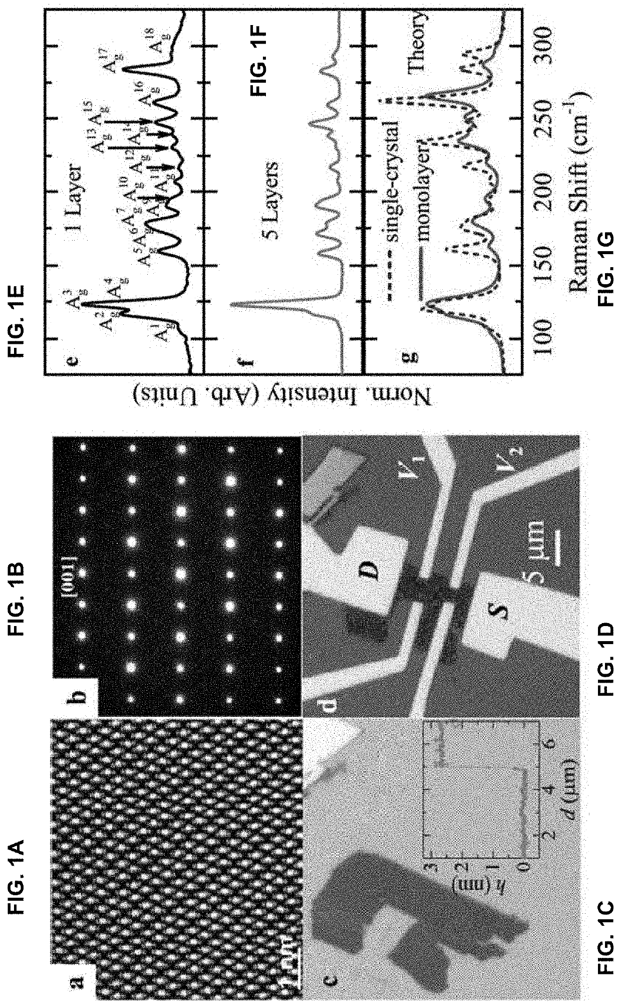
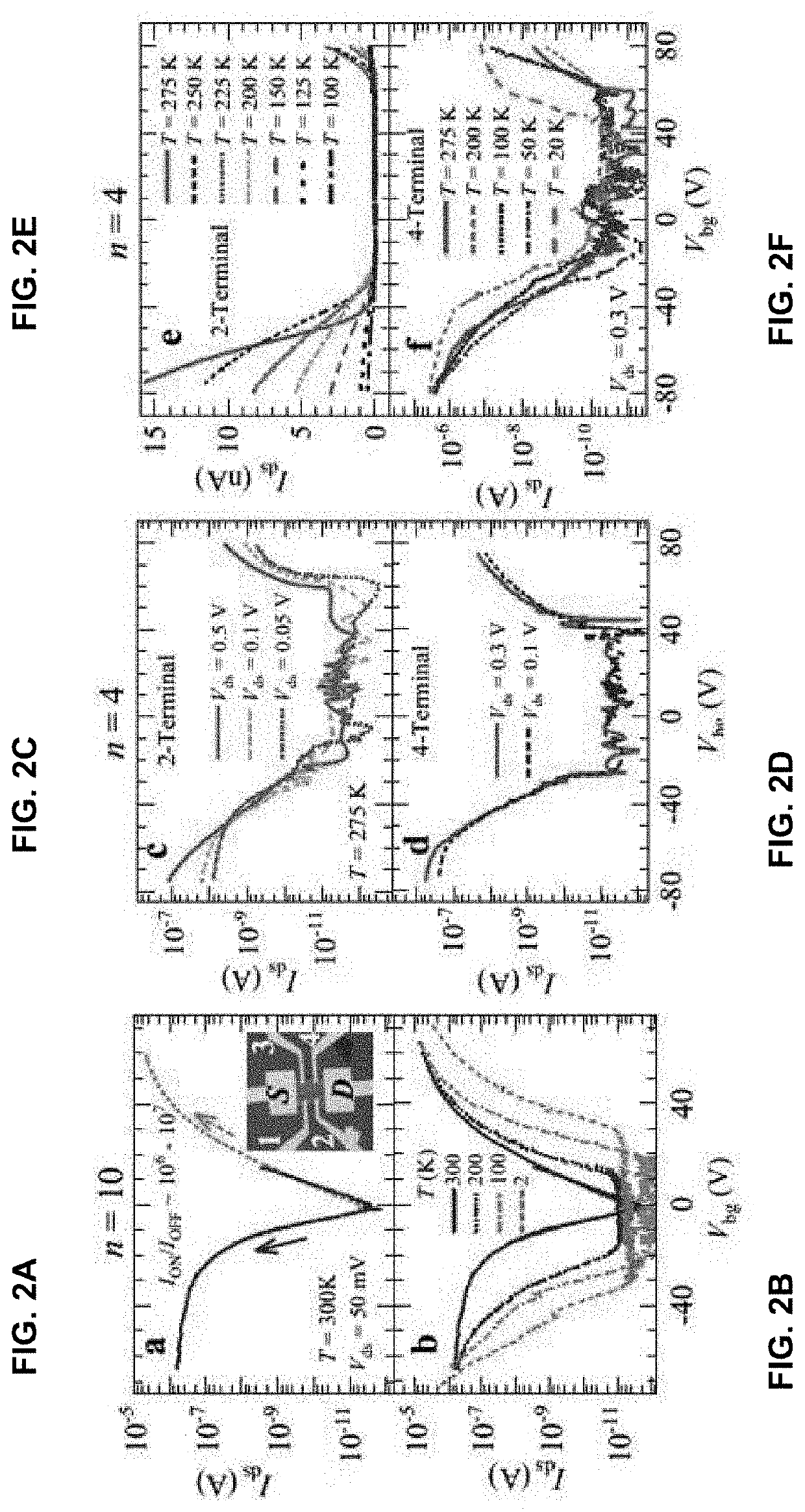
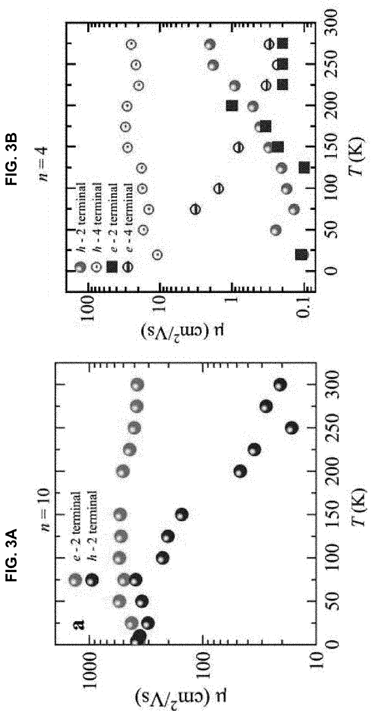
  • Phase modulators based on ambipolar field-effect transistors
  • Phase modulators based on ambipolar field-effect transistors
  • Phase modulators based on ambipolar field-effect transistors

Examples


Embodiment Construction

[0037]It will be readily understood that the components of the embodiments as generally described herein and illustrated in the appended figures could be arranged and designed in a wide variety of different configurations. Thus, the following more detailed description of various embodiments, as represented in the figures, is not intended to limit the scope of the present disclosure, but is merely representative of various embodiments. While the various aspects of the embodiments are presented in drawings, the drawings are not necessarily drawn to scale unless specifically indicated.

[0038]The present solution may be embodied in other specific forms without departing from its spirit or essential characteristics. The described embodiments are to be considered in all respects only as illustrative and not restrictive. The scope of the present solution is, therefore, indicated by the appended claims rather than by this detailed description. All changes which come within the meaning and ra...


PUM

PropertyMeasurementUnit
step heightaaaaaaaaaa
widthaaaaaaaaaa
widthaaaaaaaaaa

Abstract

Systems and methods for providing a phase modulator. The methods comprise creating a Field Effect Transistor (FET) by: placing a crystal structure displaying ambipolarity on a substrate comprising an oxide layer and a conductive silicon layer, the conductive silicon layer providing a gating electrical contact for the phase modulator, and forming source and drain electrical contacts on the crystal structure using e-beam lithography and an e-beam evaporator. The methods also comprising: annealing the FET to improve an interface between the crystal structure and the source and drain electrical contacts; and coating the FET with a dielectric layer to reduce or eliminate hysteresis so that a functionality of the phase modulator is improved.

Description

CROSS-REFERENCE TO RELATED APPLICATIONS[0001]The present application claims the benefit of U.S. Patent Application Ser. No. 62 / 741,020, filed on Oct. 4, 2018. The forgoing U.S. Patent Application is hereby incorporated by reference in its entirety.RESEARCH AND DEVELOPMENT[0002]This invention was made with government support under Grant No. W911NF-11-1-0362 awarded by the US Army Research Office and Grant No. DMR-1229217 awarded by the National Science Foundation. The government has certain rights in this invention.BACKGROUNDStatement of the Technical Field[0003]The present disclosure relates generally to phase modulators. More particularly, the present disclosure relates to phase modulators based on ambipolar field-effect transistors (“FETs”).Description of the Related Art[0004]Conventional phase modulators are made from relatively thick, non-flexible, non-transparent silicon that is not suitable for high-density, portable low-power consumption electronics. The architecture of the c...

Claims


Application Information

Patent Timeline
Patent Type & Authority Applications(United States)
IPC IPC(8): H01L29/76H01L21/02H01L21/477H01L29/66H01L29/24
CPCH01L21/02631H01L21/477H01L29/24H01L21/0262H01L21/02568H01L29/66969H01L29/7606H01L21/02694H01L29/778H01L29/78696H01L29/78681H01L23/3171H01L21/443
Inventor PRADHAN, NIHAR R.MCGILL, STEPHEN A.
Owner FLORIDA STATE UNIV RES FOUND INC
Learn More