
High Speed Switching Circuit Configuration

Inactive Publication Date: 2020-04-30
EXCELITAS CANADA
View PDF4 Cites 2 Cited by
  • Summary
  • Abstract
  • Description
  • Claims
  • Application Information

AI Technical Summary

Benefits of technology

The present invention provides a high speed switching circuit that has low inductance and is suitable for high-density connections. The circuit includes a substrate with multiple through-substrate vias and a capacitor and sink arrangement for controlled current pulses. This arrangement allows for faster and more efficient data switching with reduced latency and improved reliability.

Problems solved by technology

Presently, circuit layouts for such circuits are inadequate for a switching circuit 100 to produce pulses meeting specific amplitude and time duration specifications.

Method used


Image

  • High Speed Switching Circuit Configuration
  • High Speed Switching Circuit Configuration
  • High Speed Switching Circuit Configuration

Examples


Embodiment Construction

[0017]Reference will now be made in detail to embodiments of the present invention, examples of which are illustrated in the accompanying drawings. Wherever possible, the same reference numbers are used in the drawings and the description to refer to the same or like parts.

[0018]As used within this disclosure, a “lateral” or “horizontal” current path refers to a direction of current along the surface of a circuit board, for example through circuit board traces. A “vertical” current path refers to a direction of current substantially normal to the surface of a circuit board, for example, a current path traveling through a circuit board from a circuit board top surface to a circuit board bottom surface using a through via. As used herein, “substantially” means “very nearly,” or within typical manufacturing tolerances.

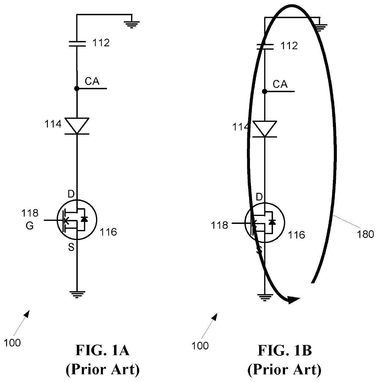
[0019]As noted in the background section above, FIG. 1A is a prior art circuit diagram of a switching circuit with components including the capacitor 112, the sink 114 (a...


PUM


Abstract

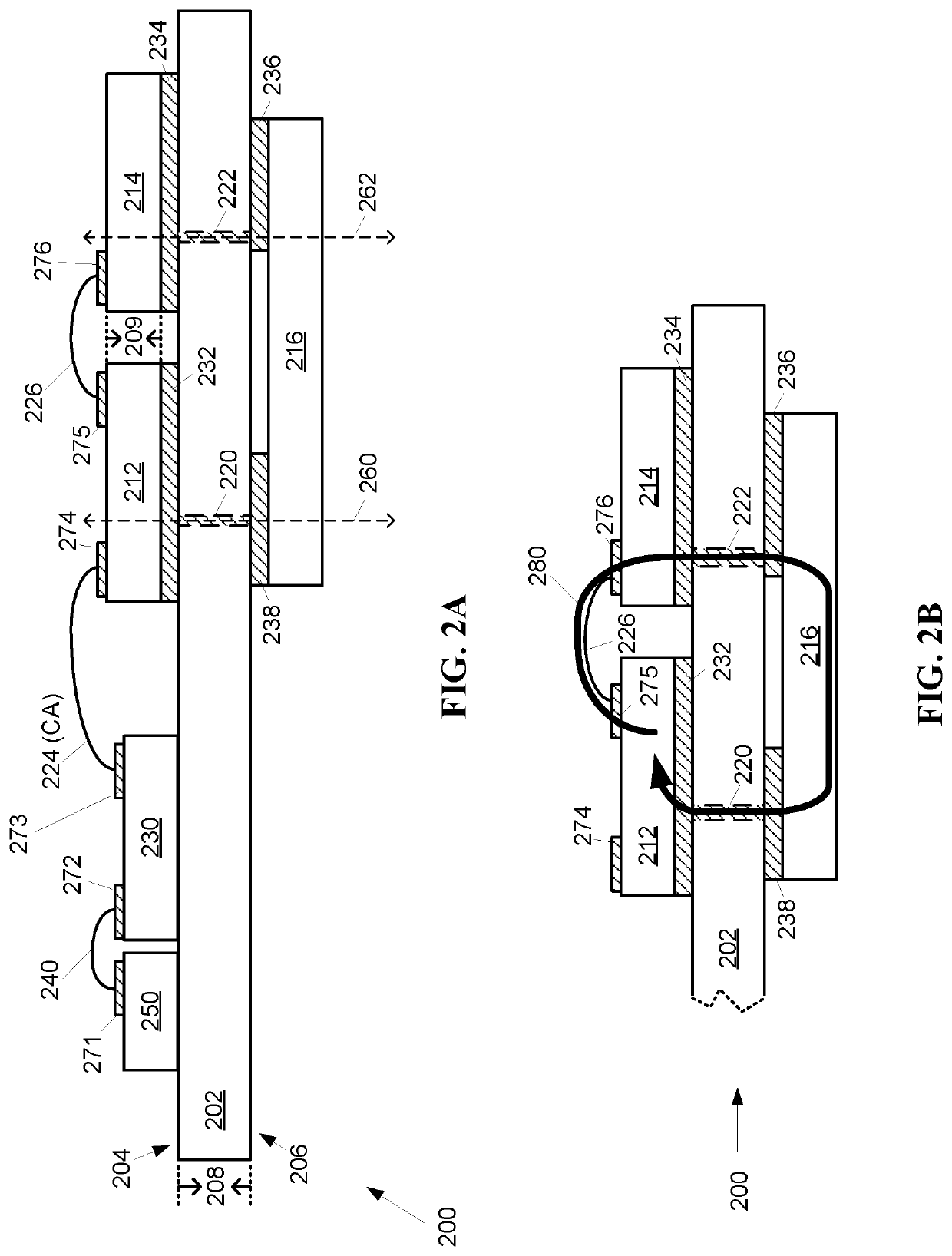
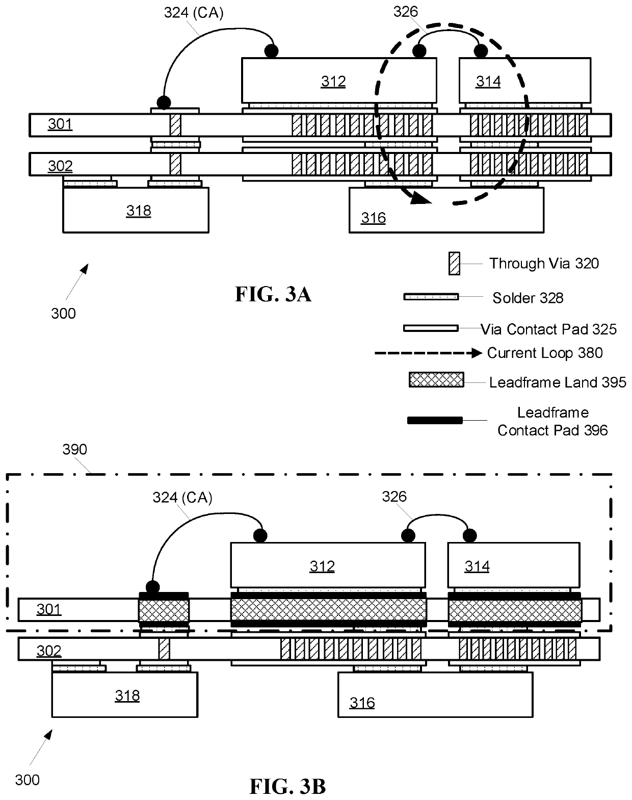
A low inductance electrical switching circuit arrangement, includes a two sided substrate with a plurality of through-substrate electrical vias. A capacitor is arranged on the substrate first side above a first via, and an electrical sink is arranged on the first side above a second via. A switching component configured to produce a plurality of current pulses is arranged on the substrate second side below the first and second via.

Description

CROSS-REFERENCE TO RELATED APPLICATIONS[0001]This application claims the benefit of U.S. Provisional Patent Application Ser. No. 62 / 752,460, filed Oct. 30, 2018, entitled “High Speed Switching Circuit Configuration,” which is incorporated by reference herein in its entirety.FIELD OF THE INVENTION[0002]The present invention relates to electronic circuitry, and more particularly, is related to a high speed switching circuit.BACKGROUND OF THE INVENTION[0003]FIG. 1A shows a basic switching circuit 100 where an electronic switch 116 having a drain D and a source S is connected across a load (or sink 114), to a capacitor 112. The capacitor 112 may be charged via a connection CA. Access to the capacitor 112 herein is represented through the connection CA. Presently, circuit layouts for such circuits are inadequate for a switching circuit 100 to produce pulses meeting specific amplitude and time duration specifications. The physical layout of the circuit elements affects the performance whe...

Claims


Application Information

Patent Timeline
IPC IPC(8): H03K17/687H01L23/495H01L23/48H05K1/16H05K1/11H05K7/20H01S5/0231
CPCH03K17/687H05K1/162H01L23/49589H01L23/481H05K7/2039H05K1/115H05K1/025H05K1/181H05K2201/066H05K2201/0792H05K2201/10015H05K2201/10106H05K2201/10166H03K17/04163H01L2224/48227H01L2224/73265H01L2224/48091H01L2224/48137Y02P70/50H01S5/0231H01L2924/00014H01S5/042H01S5/40H05K3/303H05K2201/10121H05K2201/10636H05K2201/10719H01S5/02234H01S5/02325H01S5/02345
Inventor GODFREY, LAWRENCE
Owner EXCELITAS CANADA
Learn More