Display panel and display method

Active Publication Date: 2020-05-14
XIANYANG CAIHONG OPTOELECTRONICS TECH CO LTD
View PDF0 Cites 5 Cited by
  • Summary
  • Abstract
  • Description
  • Claims
  • Application Information

AI Technical Summary

Benefits of technology

[0026]Compared with the prior art, the embodiment of the present invention can achieve one or more of the following beneficial effects:
[0027]1. The display panel of the embodiment of the present invention has a plurality of photo sensors disposed on the thin film transistor array substrate, when the incident laser is irradiated onto the photo sensor, the photo sensor can be triggered to work to determine the laser projection position to change the gray scale of the sub-pixel of the laser irradiation region, thereby improving the demonstration effect.
[0028]2. The display panel of the embodiment of the invention performs the photoelectric signal position test between the frame and the frame, that is, when the scanning signal and the control signal are both at low levels, which can well determine the laser projection position and ensure the norma

Problems solved by technology

It will cause the viewer and the user to see the highlights of the laser pen projected onto the

Method used


Image

  • Display panel and display method
  • Display panel and display method
  • Display panel and display method

Examples


embodiment 1

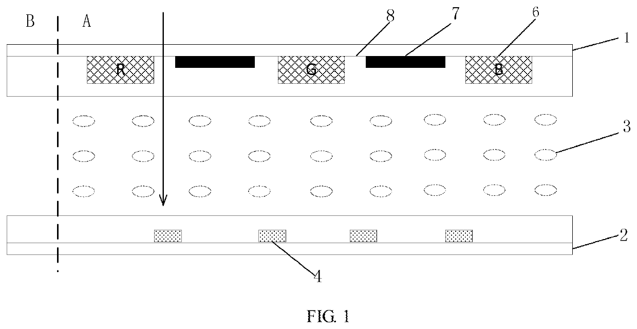
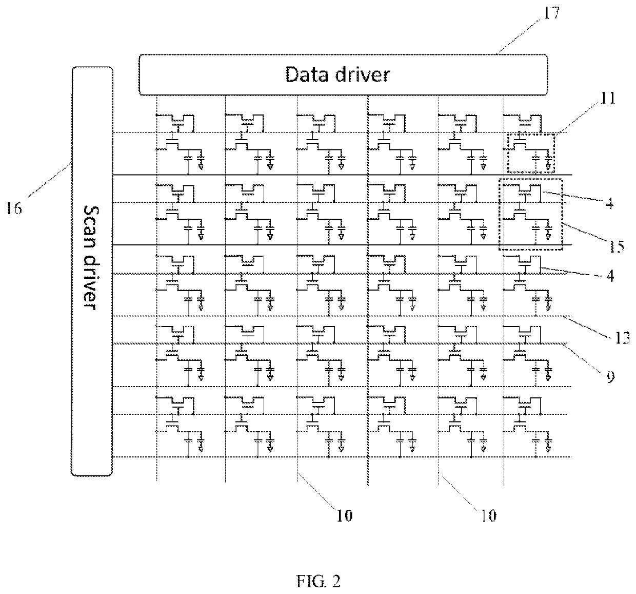
[0042]Referring to FIG. 1, FIG. 1 is a schematic structural diagram of a display panel according to an embodiment of the present invention. As shown in FIG. 1, the display panel of the embodiment can recognize external light, and includes a color filter substrate 1 and a thin film transistor array substrate 2 disposed opposite to each other, and a liquid crystal layer 3 filled between the color filter substrate 1 and the thin film transistor array substrate 2.

[0043]Further, the color filter substrate 1 includes the color filter 6 and the black matrix 7 which are arranged in phase. The light transmissive passages 8 may be formed in the color filter 6, the black matrix 7, and the color filter substrate 1 between the color filter 6 and the black matrix 7. As shown in FIG. 1, in this embodiment, the light transmissive passage 8 is formed on the color filter substrate 1 between the color filter 6 and the black matrix 7, and the photo sensor 4 is located on the thin film transistor array ...

embodiment 2

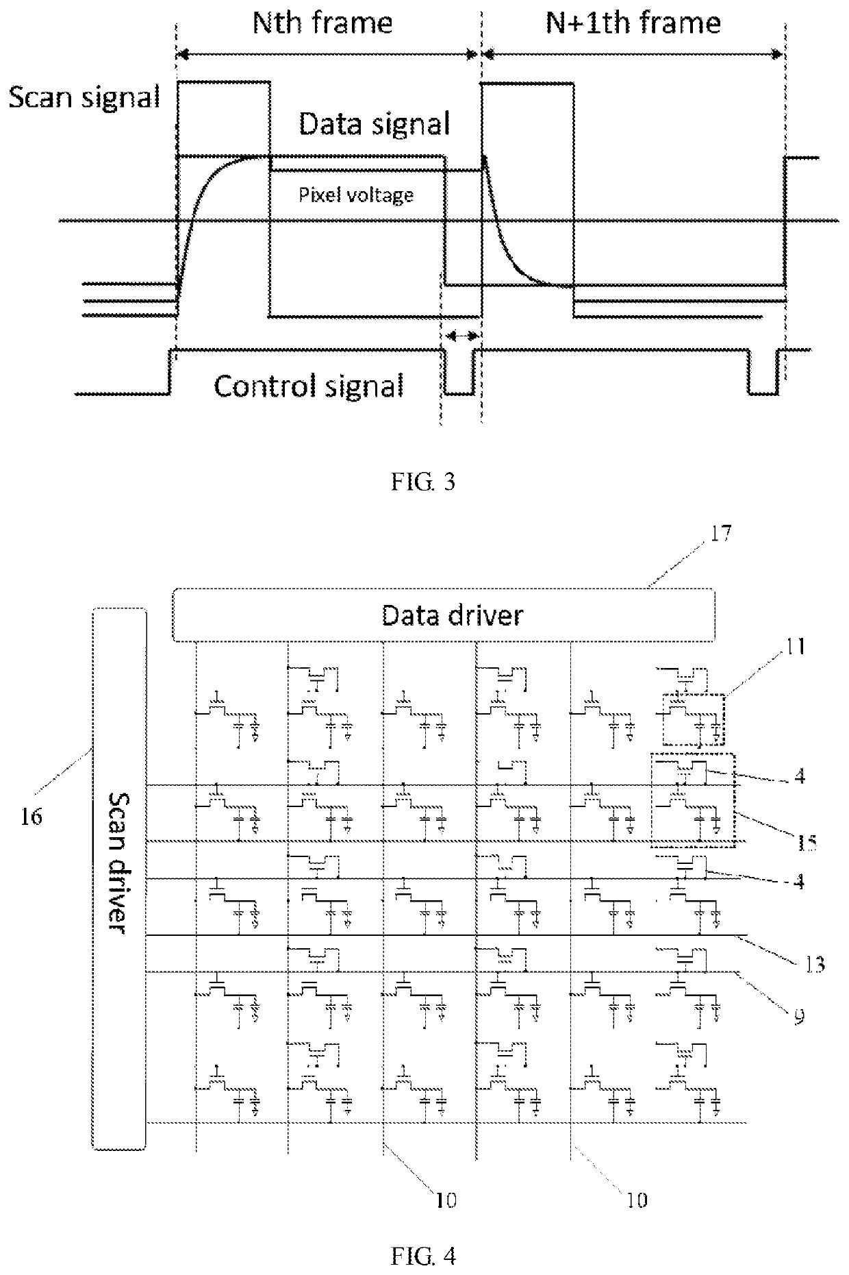
[0056]Based on the foregoing Embodiment 1, the embodiment provides a display method. Referring to FIG. 5, FIG. 5 is a flowchart of a display method according to an embodiment of the present invention. The display method of this embodiment includes:

[0057]S1: Stopping loading the common voltage to the sub-pixels in the preset period.

[0058]Specifically, in this embodiment, the preset period is a period in which the scan signal and the data signal are both al low levels. That is, as described above, in order not to affect the normal display, the photoelectric signal position test is performed between the frame and the frame, that is, when the scanning signal and the control signal are both at low levels.

[0059]S2: Detecting position information corresponding to an external photoelectric signal that is irradiated onto a designated area of the display panel during the preset period.

[0060]Specifically, S2 includes:

[0061]S21: Receiving the external photoelectric signal and generating a feedb...

embodiment 3

[0068]Referring to FIG. 6, FIG. 6 is a schematic structural diagram of a display panel according to an embodiment of the present invention. As shown in FIG. 6, the display panel of the present embodiment includes a color filter substrate 1 and a thin film transistor array substrate 2 disposed opposite to each other, and a liquid crystal layer 3 is filled between the color filter substrate 1 and the thin film transistor array substrate 2. The thin film transistor array substrate 1 includes a display area A and a non-display area B, and the liquid crystal layer 3 is located in the display area A. Further, the thin film transistor array substrate 1 includes a display area A and a non-display area B, a plurality of photo sensors 4 are disposed in the display area A. and a plurality of control switches 5 are disposed in the non-display area B; a light transmissive passage 8 is formed at a position on the color filter substrate 2 that vertically corresponds to the photo sensor 4. A plural...


PUM


Abstract

The invention provides a display panel, including a color filter substrate and a thin film transistor array substrate disposed oppositely, and a liquid crystal layer filled between the color filter substrate and the thin film transistor array substrate, wherein the thin film transistor array substrate includes a display area, a non-display area, and a plurality of photo sensors are disposed in the display area; the color filter substrate is formed with a plurality of light transmissive passages; the thin film transistor array substrate is disposed with a plurality of sub-pixels; and the photo sensor is configured for detecting position information corresponding to an external photoelectric signal when receiving the external photoelectric signal. The display panel is provided with a plurality of photo sensors, when the incident laser light is irradiated onto the photo sensor, the photo sensor can be triggered to work, and the laser projection position is determined.

Description

FIELD OF THE DISCLOSURE[0001]The present invention relates to the field of display technologies, and in particular, to a display panel and a display method.BACKGROUND OF THE DISCLOSURE[0002]The laser pointer, also known as the laser pointer, is a pen-type transmitter that is designed to be portable, hand-friendly, and processed by a laser module (light-emitting diode). It has been widely used in e-learning, presentations, and presentations.[0003]In some application scenarios, liquid crystal display panels such as LEDs and OLEDs need to be used in conjunction with a laser pointer for better presentation. When the laser pointer is projected onto the display surface of the display panel, part of the incident light is absorbed, and on the other hand, due to the high brightness of the display panel itself. It will cause the viewer and the user to see the highlights of the laser pen projected onto the display panel, and even see the bright spots, which seriously affects the presentation e...

Claims


Application Information

Patent Timeline
IPC IPC(8): G09G3/36
CPCG09G3/3688G09G2320/0666G09G2360/144G06F3/03542G09G3/3677G09G3/3607G09G2354/00G09G2360/141G09G2320/0686G06F3/0412G06F3/04166G06F3/042G06F2203/04801G09G3/3648G09G3/3655G09G2360/14G09G2360/142
Inventor ZHU, HUANHUANWU, YUAN-LIANGCHEN, YUYEHHUANG, YUSHENGLIU, ZIHAN
Owner XIANYANG CAIHONG OPTOELECTRONICS TECH CO LTD
Why Eureka
Try Eureka