Electromagnetic wave detecting apparatus and method of setting acquisition timing of detection signal

a technology of electromagnetic wave and detection signal, applied in the field of electromagnetic wave detecting apparatus, can solve the problem of relatively complicated circuit configuration, and achieve the effect of preventing a complicated circuit configuration

Active Publication Date: 2020-06-11
PIONEER CORP
View PDF0 Cites 0 Cited by
  • Summary
  • Abstract
  • Description
  • Claims
  • Application Information

AI Technical Summary

Benefits of technology

[0005]In view of the aforementioned problem, it is therefore an object of the present invention to provide an electromagnetic wave detecting apparatus configured to appropriately apply bias voltage to each of a plurality of detecting elements while preventing a complicated circuit configuration, as well as a method of setting the acquisition timing of a detection signal.Solution to Problem

Problems solved by technology

A technology / technique described in the Patent Literature 1 requires a switch for selecting the bolometer type thermoelectric conversion element(s) which is to be supplied with the bias voltage, and for example, a circuit configuration is relatively complicated, which is technically problematic.
This problem is more evident with increasing number of the bolometer type thermoelectric conversion elements, which are detecting elements.

Method used


Image

  • Electromagnetic wave detecting apparatus and method of setting acquisition timing of detection signal
  • Electromagnetic wave detecting apparatus and method of setting acquisition timing of detection signal
  • Electromagnetic wave detecting apparatus and method of setting acquisition timing of detection signal

Examples


first practical example

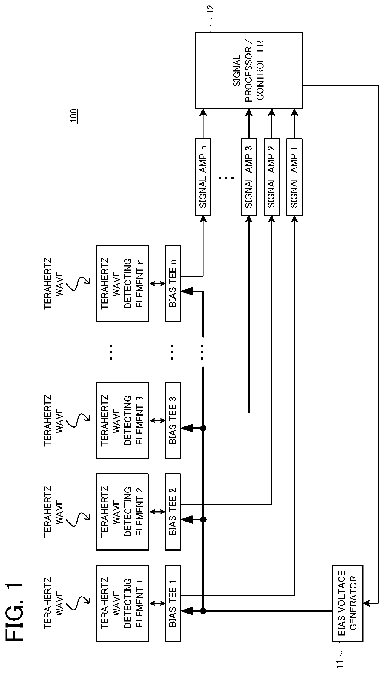
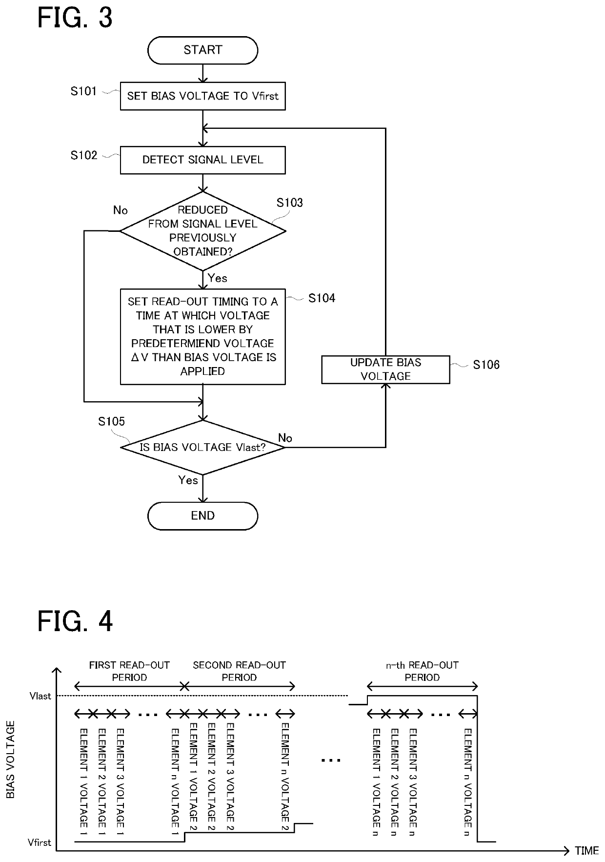
[0028]A terahertz wave detecting apparatus according to a first practical example, which is an example of the electromagnetic wave detecting apparatus according to the present invention, will be explained with reference to FIG. 1 to FIG. 3.

(Configuration of Apparatus)

[0029]A configuration of the terahertz wave detecting apparatus according to the first practical example will be explained with reference to FIG. 1. FIG. 1 is a block diagram illustrating the configuration of the terahertz wave detecting apparatus according to the first practical example.

[0030]In FIG. 1, a terahertz wave detecting apparatus 100 is provided with: a plurality of terahertz wave detecting elements 1, 2, 3, . . . , n; a plurality of bias tee circuits 1, 2, 3, . . . , n, which are respectively electrically connected to the terahertz wave detecting elements 1, 2, 3, . . . , n; a bias voltage generator 11 configured to apply bias voltage to each of the terahertz wave detecting elements 1, 2, 3, . . . , n, via r...

modified example

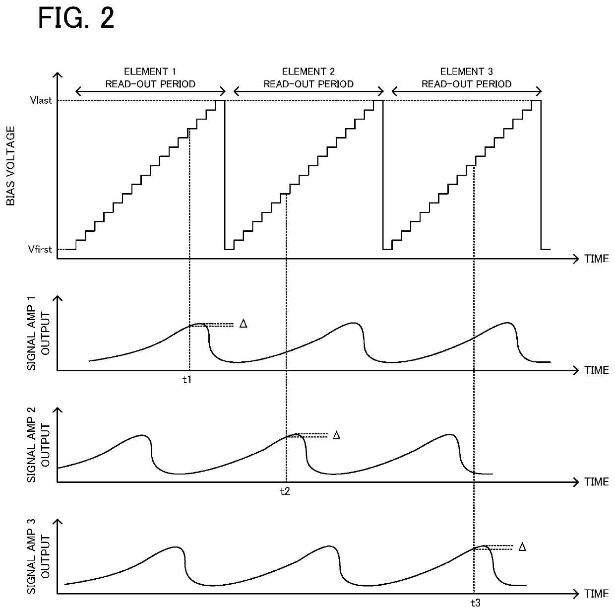
[0051]In the aforementioned first practical example, as illustrated in FIG. 2, the terahertz wave detecting element that is a sampling target is changed in every period of the sawtooth wave of the bias voltage. For example, as illustrated in FIG. 4, every time the voltage value of the bias voltage is changed, all the terahertz wave detecting elements 1, 2, 3, . . . , n may be set as sampling targets, and the detection signal from the terahertz wave detecting element whose current bias voltage is the optimum bias voltage may be actually sampled.

[0052]Moreover, in the aforementioned first practical example, the voltage that is lower by the predetermined voltage than the bias voltage that allows the maximum detection sensitivity of each terahertz wave detecting element is set as the “optimum bias voltage”. The bias voltage that allows the maximum detection sensitivity of each terahertz wave detecting element may be also set as the “optimum bias voltage”.

[0053]Moreover, the bias voltage...

second practical example

[0054]A terahertz wave detecting apparatus according to a second practical example, which is an example of the electromagnetic wave detecting apparatus according to the present invention, will be explained with reference to FIG. 5 and FIG. 6. The second practical example is the same as the aforementioned first practical example, except that the circuit configuration is partially different. Thus, in the second practical example, the same explanation as that in the first practical example will be omitted, as occasion demands, and the same parts on the drawings will carry the same reference numerals. An explanation will be given only to basically different points with reference to FIG. 5 and FIG. 6.

(Configuration of Apparatus)

[0055]A configuration of the terahertz wave detecting apparatus according to the second practical example will be explained with reference to FIG. 5. FIG. 5 is a block diagram illustrating the configuration of the terahertz wave detecting apparatus according to th...


PUM


Abstract

An electromagnetic wave detecting apparatus is provided with: a plurality of detecting devices each of which is configured to detect an electromagnetic wave; a voltage applying device configured to apply bias voltage to each of the plurality of detecting devices; an obtaining device configured to obtain a detection signal outputted from each of the plurality of detecting devices; and a setting device configured to set acquisition timing of the detection signal for each of the plurality of detecting devices, on the basis of the bias voltage, which is applied to each of the plurality of detecting devices, and the detection signal of each of the plurality of detecting devices.

Description

TECHNICAL FIELD[0001]The present invention relates to an electromagnetic wave detecting apparatus configured to detect an electromagnetic wave, such as, for example, a terahertz wave, and a method of setting acquisition timing of a detection signal on the electromagnetic wave detecting apparatus.BACKGROUND ART[0002]For this type of apparatus, for example, there is proposed a level adjusting circuit for an infrared sensor, which is configured to selectively supplying bias voltage to each of a plurality of bolometer type thermoelectric conversion elements, which are arranged in a grid, from a constant voltage bias circuit, thereby selectively reading out an electric current that flows in each of the bolometer type thermoelectric conversion elements, and obtaining data about each of the bolometer type thermoelectric conversion elements (refer to Patent Literature 1). The Patent Literature 1 describes that the level adjusting circuit is provided with: a storage configured to store there...

Claims


Application Information

Patent Timeline
Patent Type & Authority Applications(United States)
IPC IPC(8): G01J1/44
CPCG01J1/44G01J2001/4426G01J2001/4446G01J3/42G01J2005/202G01J5/24G01J2005/106G01J2001/4406G01J2001/446G01R29/0871G01R29/0814
Inventor TANAKA, HIROYUKI
Owner PIONEER CORP
Why Eureka
Try Eureka