

Three-dimensional image element and optical radar device
a three-dimensional image and optical radar technology, applied in the direction of reradiation, distance measurement, instruments, etc., can solve the problems of increased size and high cost of scanning types, and achieve the effect of low cos
- Summary
- Abstract
- Description
- Claims
- Application Information
AI Technical Summary
Benefits of technology
Problems solved by technology
Method used
Image

Examples
embodiment 1
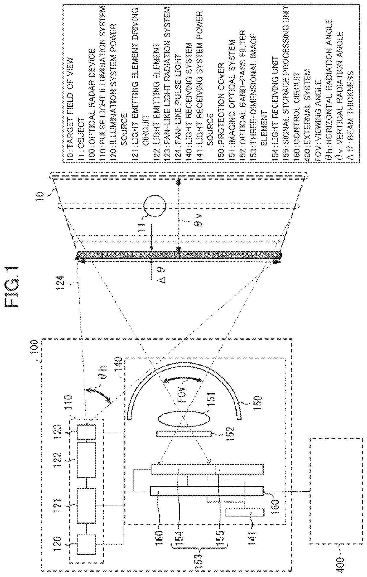
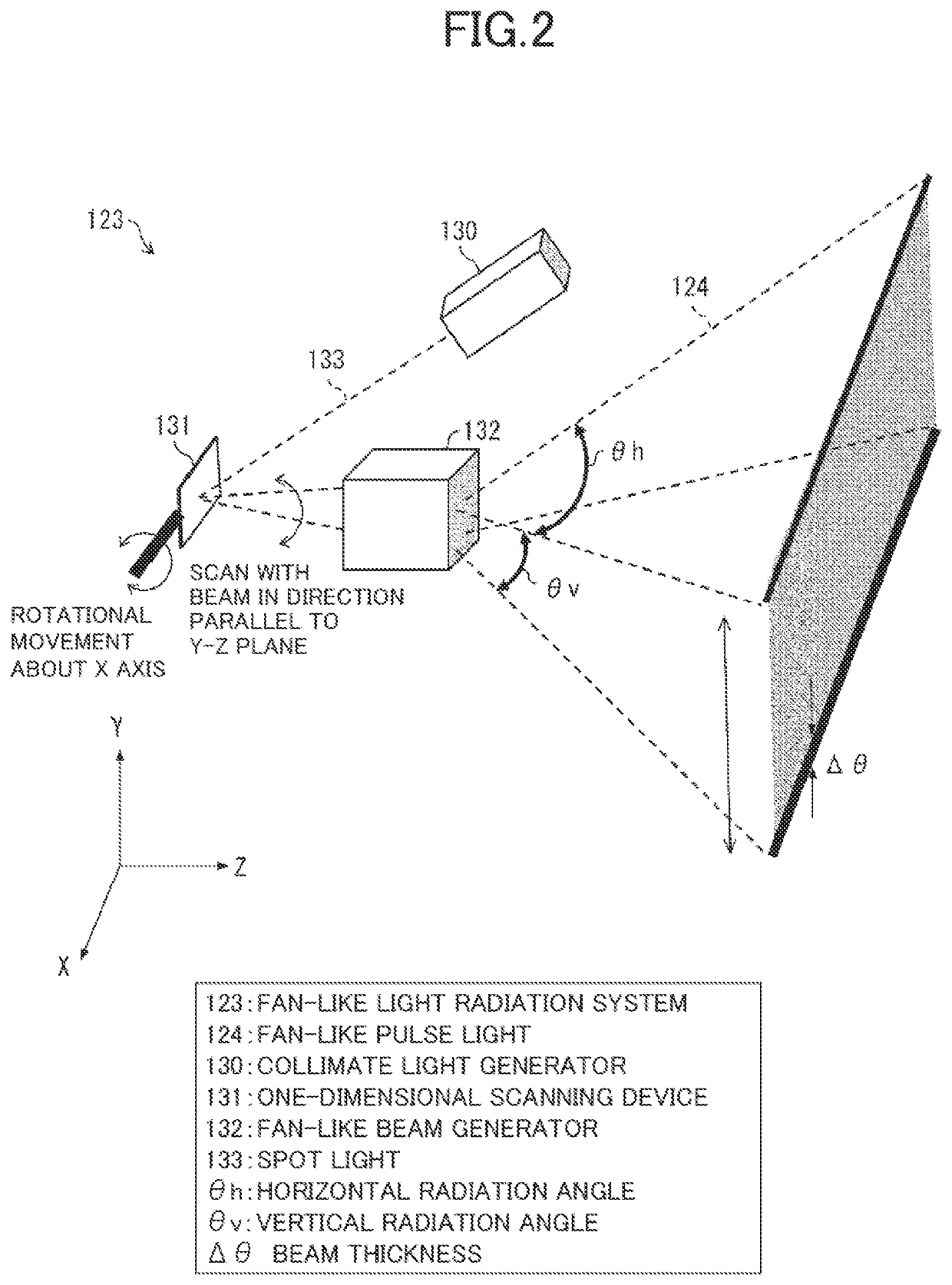
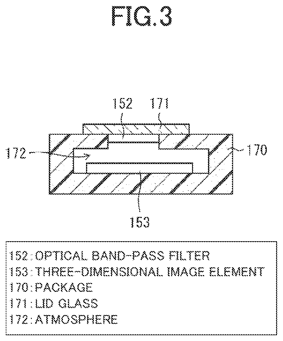
[0036]An optical radar device 100 according to Embodiment 1 of the invention will be described with reference to FIGS. 1 to 11. The optical radar device 100 includes a pulse light illumination system 110 that has a light emitting element 122 that emits pulse light, a one-dimensional scanning device (optical scanning unit) 131 that performs scanning with the pulse light in a direction parallel to a first plane, and a fan-like beam generator (optical conversion unit) 132 that converts the pulse light used for scanning by the one-dimensional scanning device 131 into fan-like pulse light 124 that is spread in a direction vertical to the first plane, and an imaging optical system 151 that images and projects light, which is from at least a part of a target field of view (region where light is radiated from the pulse light illumination system) 10, onto a light receiving unit 154 of a three-dimensional image element (sensor) 153, which measures at least a distance to an object 11, through ...
embodiment 2
[0116]The present embodiment is the same as Embodiment 1 other than a difference that in measurement of each line (row), pulse light is radiated by changing power thereof in two stages so that a part at a close distance is firstly measured through radiation with low power and a whole is then measured with high power.
[0117]As described in Embodiment 1, the intensity of the pulse light is too high at the close distance and the light receiving system 140 is saturated so that correct distance measurement is not able to be performed. Thus, the intensity of the pulse light is firstly reduced to 10 W and integration measurement is performed ten times, and then, integration is performed 140 times with the power of 75 W similarly to Embodiment 1. After the integration for the first ten times, data accumulated in the pixel storage element Mx(j) is copied to the buffer memory Bx(j) and data processing is performed for the data in the buffer memory Bx(j). Distance data that is obtained is store...
embodiment 3
[0126]FIG. 12 is a schematic view of the three-dimensional image element 153 according to the present embodiment. FIG. 13 is a schematic view illustrating connection of the pixel Px(i,j), signal lines Lxa(j) to LxC(j), and pixel storage elements Mxa(j) to MxC(j) of the three-dimensional image element 153 according to the present embodiment.
[0127]A substantial difference of the present embodiment from Embodiment 1 is that a plurality of pixel storage elements Mx(j) are provided so that data of a plurality of pixels that are adjacent is able to be measured at the same time. In an example of FIG. 12, each column has three pixel storage elements Mxa(j), Mxb(j), and MxC(j). In a case where accuracy of angle control of the one-dimensional scanning device 131 is low and correspondence between fan-like pulse light 124-α and a pixel Px(α,j) is disturbed, the beam thickness Δθ is inevitably increased to increase a margin in the configuration of Embodiment 1. However, this causes reduction of ...
PUM
 Abstract
Description
Claims
Application Information