

Fowbcsp chip module with packaging structure and manufacturing method of the same
- Summary
- Abstract
- Description
- Claims
- Application Information
AI Technical Summary
Benefits of technology
Problems solved by technology
Method used
Image

Examples
Embodiment Construction
[0045]In order that those skilled in the art can further understand the present invention, a description will be provided in the following in details.
[0046]However, these descriptions and the appended drawings are only used to cause those skilled in the art to understand the objects, features, and characteristics of the present invention, but not to be used to confine the scope and spirit of the present invention defined in the appended claims.
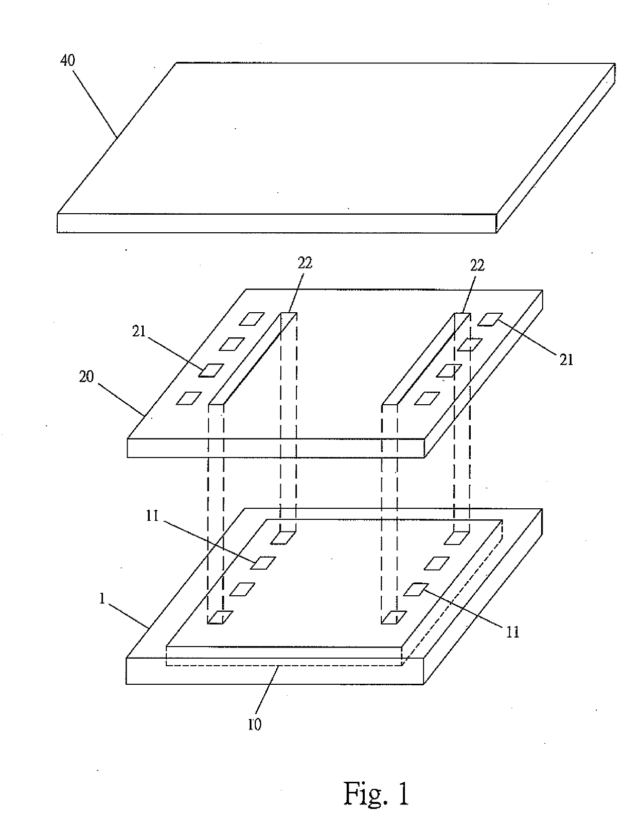
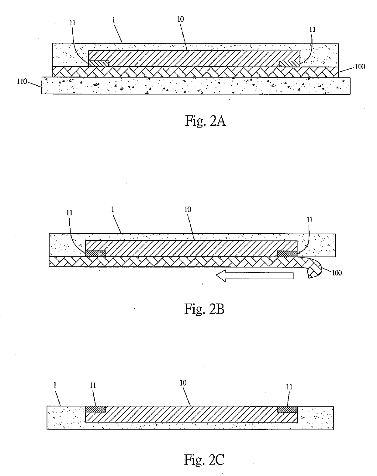
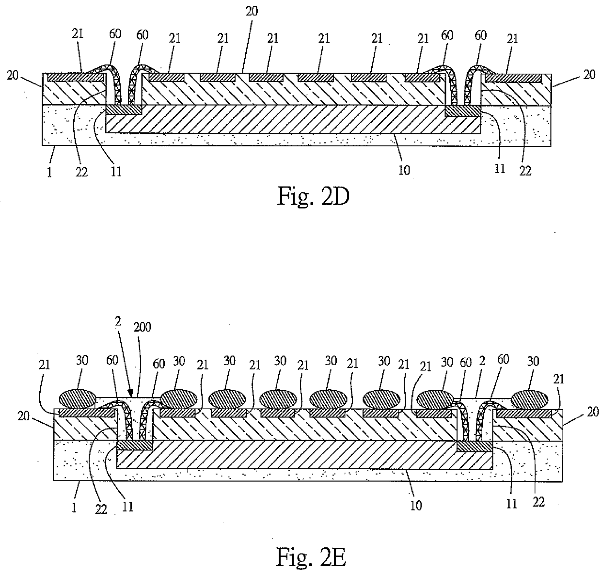
[0047]With reference to FIGS. 1 to 2F, and 11, the first embodiment of the present invention is illustrated. The first embodiment in the present invention includes the following steps of:
[0048]Step A: as shown in FIG. 2A, taking a chip 10; a lower side of the chip 10 having a plurality of joints 11; taking a non-adhesive film 100 to be on the lower side of the chip 100; then taking a supporting plate 110 to be under the non-adhesive film 100; forming a first packaging structure 1 to enclose an upper side and lateral sides of the chip 10 so as ...
PUM
 Abstract
Description
Claims
Application Information