

Chip carrier and chip package structure thereof
- Summary
- Abstract
- Description
- Claims
- Application Information
AI Technical Summary
Benefits of technology
Problems solved by technology
Method used
Image

Examples
Embodiment Construction
[0024] Reference will now be made in detail to the present preferred embodiments of the invention, examples of which are illustrated in the accompanying drawings. Wherever possible, the same reference numbers are used in the drawings and the description to refer to the same or like parts.
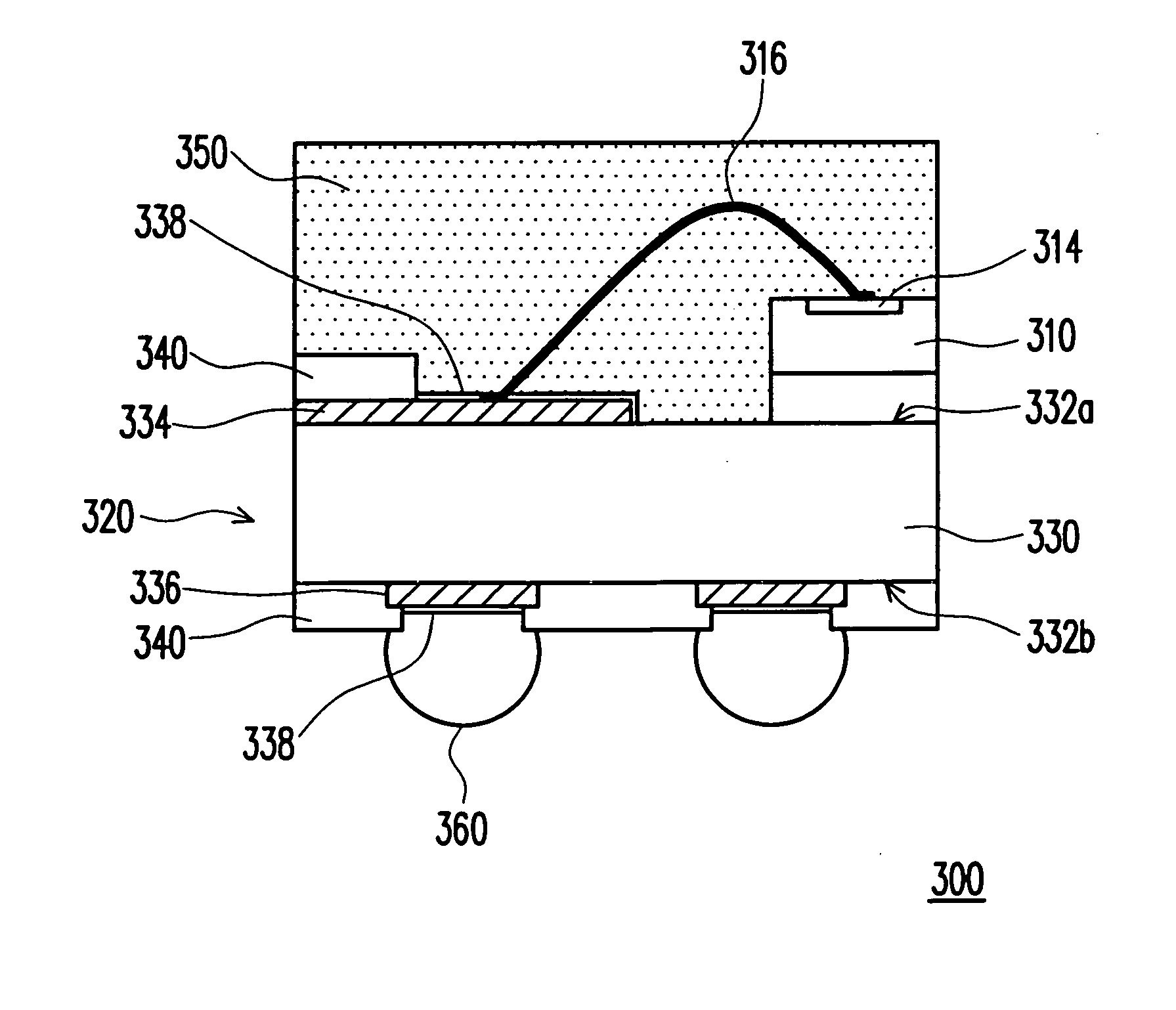
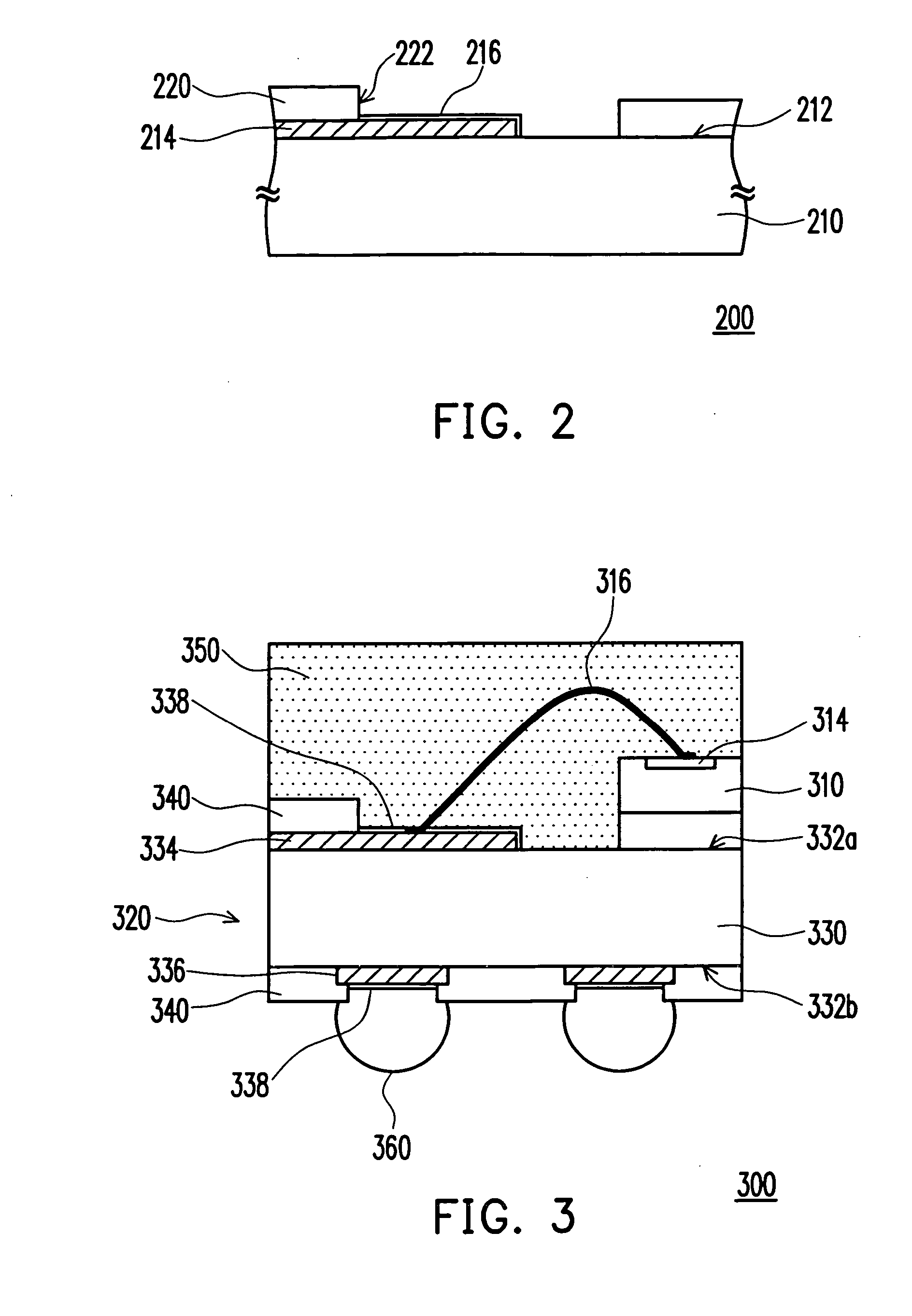
[0025]FIG. 2 is a schematic cross-sectional view showing part of a chip carrier according to one preferred embodiment of the present invention. As shown in FIG. 2, the chip carrier 200 is an organic dielectric substrate, an inorganic dielectric substrate or a flexible circuit board, for example. The chip carrier 200 comprises a laminated layer 210, an oxidation protection layer 216 and a solder mask layer 220. The laminated layer 210 comprises at least a patterned conductive layer and at least a dielectric layer. In a multi-layered circuit board, for example, the dielectric layer is disposed between two neighboring patterned conductive layers. The patterned conductive layers can be electrically con...
PUM
 Abstract
Description
Claims
Application Information