

Display panel, display panel inspection method, and display panel manufacturing method
- Summary
- Abstract
- Description
- Claims
- Application Information
AI Technical Summary
Benefits of technology
Problems solved by technology
Method used
Image

Examples
embodiment 1
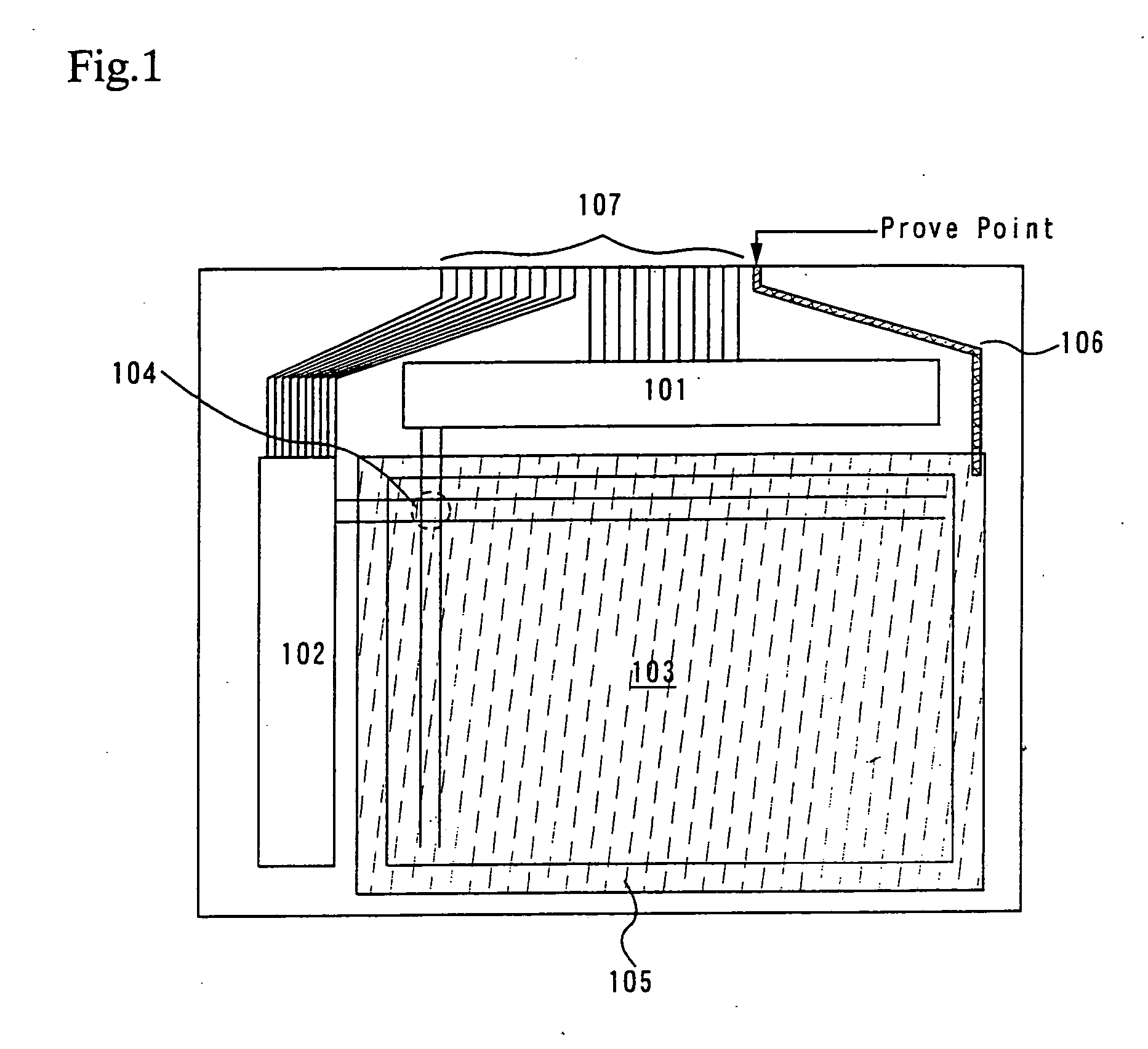
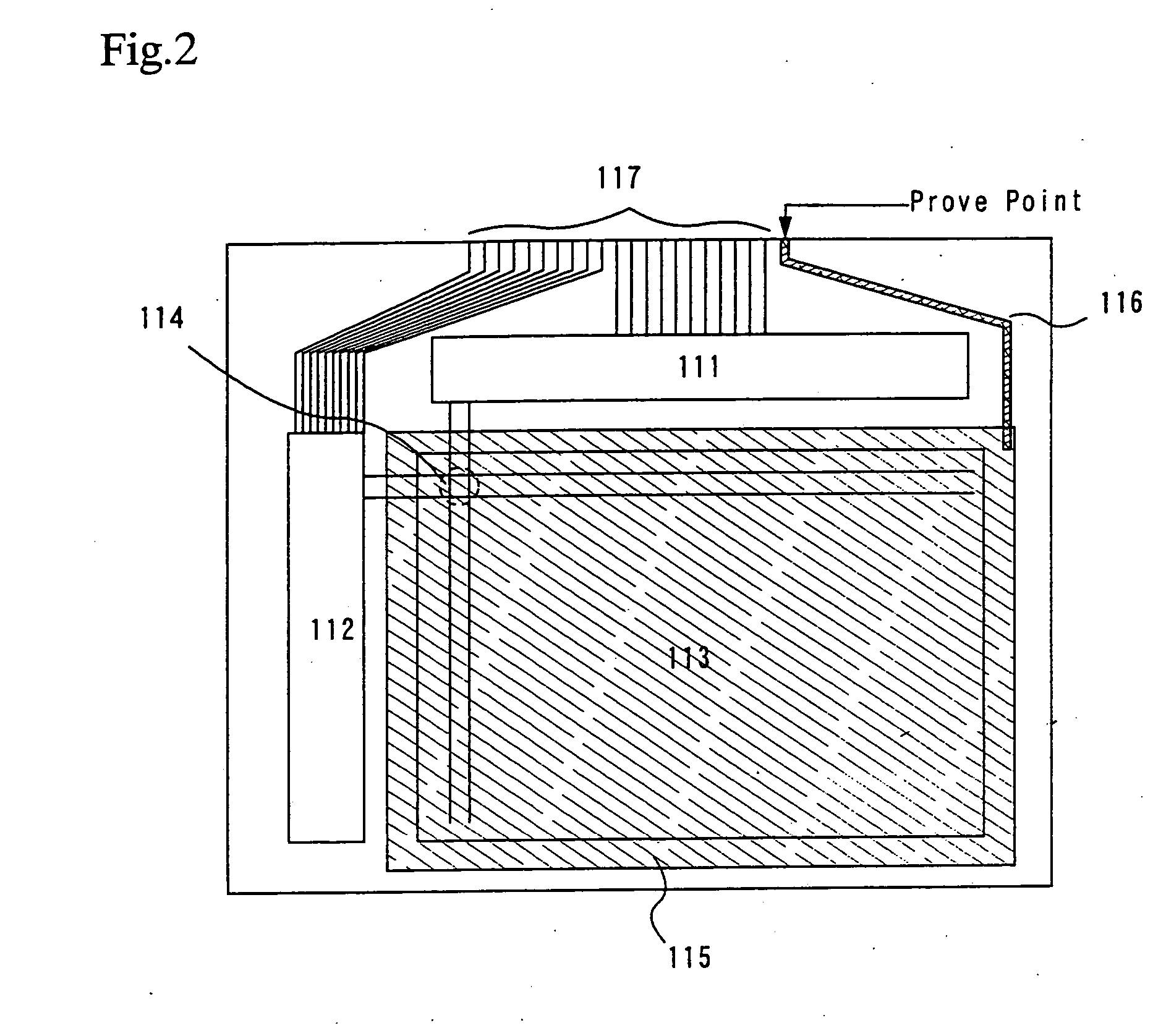
[0107] An example of applying the inspection method of the present invention to an EL panel comprising a pixel portion with a different structure from the EL panel shown in the embodiment mode is explained in embodiment 1.
[0108] A circuit diagram of a pixel portion 501 of an EL panel used in embodiment 1 is shown in FIG. 6. In embodiment 1, a region which has any one of first gate signal lines Ga1 to Gay, any one of second gate signal lines Ge1 to Gey, any one of the source signal lines S1 to Sx, and any one of the electric power source supply lines V1 to Vx, is a pixel 502. A plurality of pixels 502 are arranged in a matrix shape in the pixel portion 501.
[0109] Any one of the first gate signal lines Ga1 to Gay to which a first selection signal is input from a first gate signal line driver circuit is connected to a gate electrode of a first switching TFT 503 of each pixel 502. Further, one of a source region and a drain region of the first switching TFT 503 of each pixel is connec...
embodiment 2
[0144] An example of a top surface diagram of a pixel of an EL panel after inspection using the inspection method of the present invention is shown in embodiment 2.
[0145]FIG. 9A shows a top surface diagram of a pixel in the embodiment 2, and FIG. 9B shows a circuit diagram of the pixel. Reference numeral 4402 denotes a switching TFT, and reference numeral 4406 denotes an EL driver TFT.
[0146] The switching TFT 4402 has gate electrodes 4404a and 4404b, portions of a gate signal line 4404. A source region of the switching TFT 4402 is connected to a source signal line 4415, and a drain region of the switching TFT 4402 is connected to a drain wiring 4405. Further, the drain wiring 4405 is electrically connected to a gate electrode 4407 of the EL driver TFT 4406. A source region of the EL driver TFT 4406 is electrically connected to an electric power source supply line 4416, and a drain region of the EL driver TFT 4406 is electrically connected to a drain wiring 4417. In addition, the d...
embodiment 3
[0150] In the EL panel shown in FIG. 5, a method of manufacturing a pixel portion, and TFTs (n-channel TFTs and p-channel TFTs) of a driver circuit provided in the periphery of the pixel portion, on the same substrate at the same tome, applying the first method of inspection, is explained in detail in Embodiment 3.
[0151] First, as shown in FIG. 10A, a base film 401 made of an insulating film such as a silicon oxide film, a silicon nitride film, or a silicon oxynitride film is formed on a substrate 400 made from glass, such as barium borosilicate glass or aluminum borosilicate glass, typically Corning Corp. #7059 glass or #1737 glass, or quartz. For example, a silicon oxynitride film manufactured from SiH4, NH3, and N2O by plasma CVD is formed with a thickness of 10 to 200 nm (preferably from 50 to 100 nm), and a hydrogenated silicon oxynitride film with a thickness of 50 to 200 nm (preferably between 100 and 150 nm), manufactured from SiH4 and N2O, is similarly formed and laminated...
PUM
 Abstract
Description
Claims
Application Information