Differential amplifier circuit
a technology of amplifier circuit and output voltage, which is applied in the direction of differential amplifier, amplifier with semiconductor device/discharge tube, amplifier details, etc., can solve the problems of difficult to obtain the desired output voltage, and the characteristics of the two fets may not be completely identical, so as to reduce the variation of output voltage
- Summary
- Abstract
- Description
- Claims
- Application Information
AI Technical Summary
Benefits of technology
Problems solved by technology
Method used
Image

Examples
first embodiment
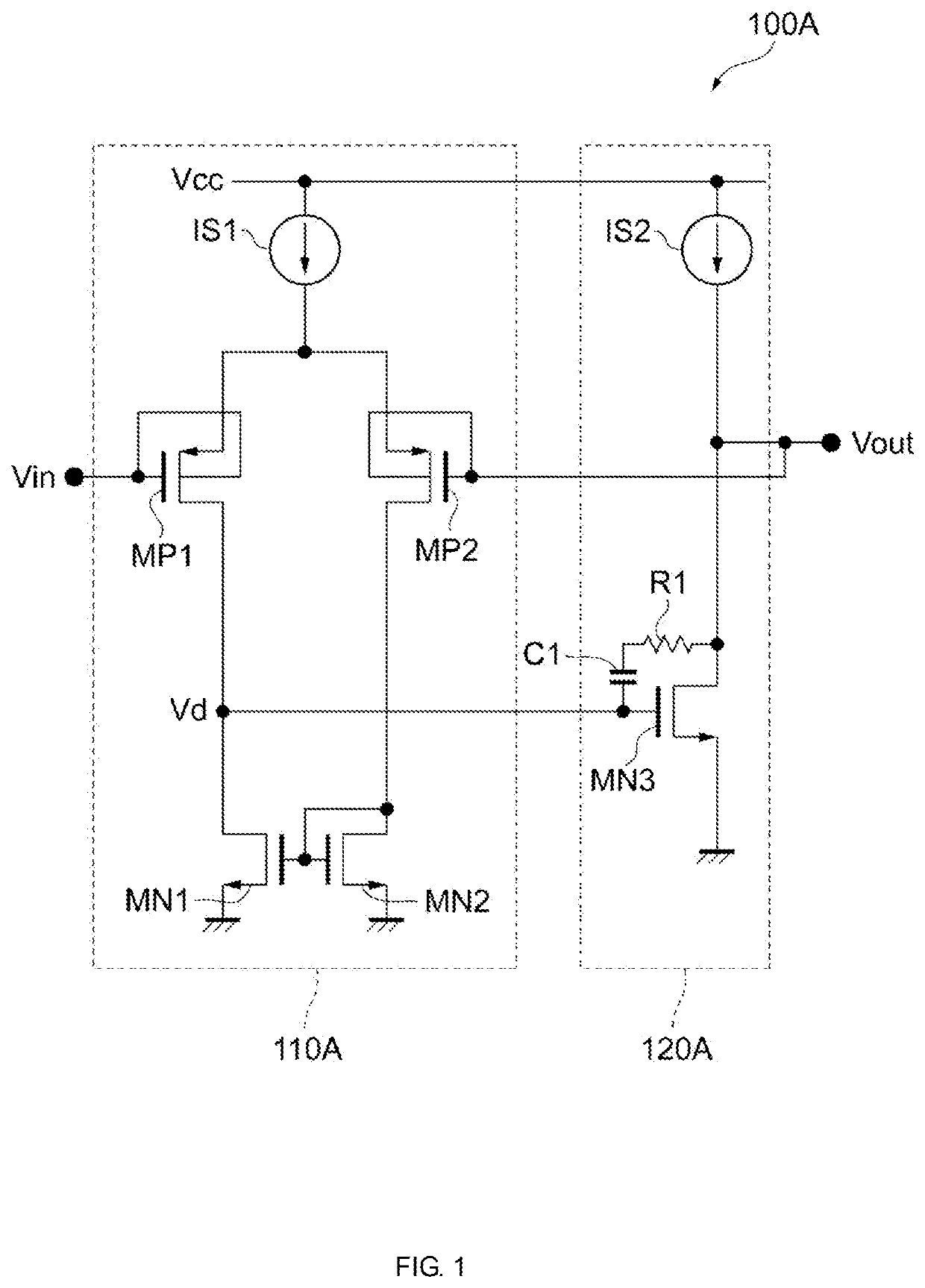
[0019]FIG. 1 is a circuit diagram illustrating the configuration of a differential amplifier circuit 100A according to the present disclosure. The differential amplifier circuit 100A illustrated in FIG. 1 constitutes a so-called voltage follower circuit. Specifically, the differential amplifier circuit 100A includes an initial-stage circuit 110A and an output circuit 120A, and the initial-stage circuit 110A includes a differential pair. The initial-stage circuit 110A includes, for example, P-channel metal oxide semiconductor field-effect transistors (MOSFETs) (MP1 and MP2), N-channel MOSFETs (MN1 and MN2), and a current source IS1. The output circuit 120A includes an N-channel MOSFET (MN3), a current source IS2, a resistor element R1, and a capacitor C1. The individual components will be described specifically.
[0020]The P-channel MOSFETs (MP1 and MP2) constitute a differential pair. Specifically, the P-channel MOSFET (MP1) (first FET) has a source connected to a source of the P-chan...
third embodiment
[0044]FIG. 5 is a circuit diagram illustrating the configuration of a differential amplifier circuit 100C according to the present disclosure. Unlike the differential amplifier circuit 100B illustrated in FIG. 4, the differential amplifier circuit 100C illustrated in FIG. 5 includes an initial-stage circuit 110C further including a level shifter circuit 130. The level shifter circuit 130 includes, for example, P-channel MOSFETs (MP6 and MP7) and current sources IS5 and IS6.
[0045]The P-channel MOSFET (MP6) (third FET) has a source connected to the gate of the N-channel MOSFET (MN4), a gate to which the input voltage Vin is input, and a drain grounded. The P-channel MOSFET (MP7) (fourth FET) has a source connected to the gate of the N-channel MOSFET (MN5), a gate to which the output voltage Vout (first feedback voltage) is input, and a drain grounded. In addition, currents generated by the current sources IS5 (second current source) and IS6 (second current source) flow between the sou...
fourth embodiment
[0050]FIG. 6 is a circuit diagram illustrating the configuration of a differential amplifier circuit 100D according to the present disclosure. The differential amplifier circuit 100D illustrated in FIG. 6 constitutes a boost regulator circuit. Specifically, unlike the differential amplifier circuit 100B, the differential amplifier circuit 100D includes an output circuit 120C including resistor elements R2 and R3 instead of the current source IS4.
[0051]The resistor elements R2 and R3 are connected in series between the drain of the P-channel MOSFET (MP5) (i.e., the terminal from which the output voltage Vout is output) and ground. Specifically, the resistor element R2 (first load) has an end connected to the drain of the P-channel MOSFET (MP5) and another end connected to an end of the resistor element R3. The resistor element R3 (second load) has another end grounded.
[0052]In this embodiment, the output voltage Vout is not input directly to the gate of the N-channel MOSFET (MN5), bu...
PUM
 Abstract
Description
Claims
Application Information
 - Generate Ideas
- Intellectual Property
- Life Sciences
- Materials
- Tech Scout
- Unparalleled Data Quality
- Higher Quality Content
- 60% Fewer Hallucinations
Browse by: Latest US Patents, China's latest patents, Technical Efficacy Thesaurus, Application Domain, Technology Topic, Popular Technical Reports.
© 2025 PatSnap. All rights reserved.Legal|Privacy policy|Modern Slavery Act Transparency Statement|Sitemap|About US| Contact US: help@patsnap.com