
Electron gun and electron beam application device

a technology of electron beam and application device, which is applied in the direction of basic electric elements, electrical discharge tubes, electrical apparatus, etc., can solve the problems of deteriorating image sharpness and increasing spot diameter, and achieves improved imaging speed, reduced roughness, and high sharpness

Active Publication Date: 2020-08-20
HITACHI HIGH-TECH CORP
View PDF0 Cites 1 Cited by
  • Summary
  • Abstract
  • Description
  • Claims
  • Application Information

AI Technical Summary

Benefits of technology

The patent is about a new technology that allows for more efficient and precise detection of target substances. This technology uses a special coating on a surface that helps to improve the performance of sensors. Its technical effects include better accuracy and reliability in detecting specific substances, which can be useful in various applications such as medical diagnostics or environmental monitoring.

Problems solved by technology

Since the size of the light source is determined by an electron source, how to reduce the aberration of the convergent lens is a problem for an electron irradiation system.
This means that when the current amount is increased in order to control the image roughness, the spot diameter increases and the image sharpness is deteriorated.

Method used


Image

  • Electron gun and electron beam application device
  • Electron gun and electron beam application device
  • Electron gun and electron beam application device

Examples


first embodiment

[0034]FIG. 3 shows a schematic diagram of an electron gun 300 according to a first embodiment and an axial magnetic field distribution 310 thereof. The electron gun 300 includes an electron source 101, an extraction electrode 102, an acceleration electrode 103, a coil 104 and a magnetic path 201 that form a control lens, and a magnetic field canceling coil 301 and a magnetic path 302.

[0035]First, since the coil 104 used in the control lens is disposed below the acceleration electrode 103, it is not necessary to remove the coil 104 when the electron gun is baked, and a vacuum start of the electron gun is easier than that in a coil detachable electron gun. In addition, since a physical position of the coil 104 and the magnetic path 105 can be adjusted independently of the extraction electrode 102 and the acceleration electrode 103 that generate an electric field, an axis of a lens generated by the electric field and an axis of a lens generated by the magnetic field can be adjusted ind...

second embodiment

[0040]FIG. 4 shows a schematic diagram of an electron gun 400 according to a second embodiment and an axial magnetic field distribution 410 thereof. A magnetic shield made of a magnetic body is disposed downstream of the extraction electrode 102 to prevent the electron source from being immersed in the magnetic field. A magnetic shield 401 is a magnetic disk having an opening for allowing the electron beam to pass through in the center. In the axial magnetic field distribution 410, calculation results of an axial magnetic field 411 when the magnetic shield 401 is not disposed and an axial magnetic field 412 when the magnetic shield 401 is disposed are shown. By disposing the magnetic shield 401, the magnetic field near the electron source can be reduced.

[0041]In order to further simplify a structure, the extraction electrode 102 can be made of a magnetic body and used as the magnetic shield instead of disposing a new magnetic shield. Such a structure can also prevent the electron so...

third embodiment

[0042]FIG. 5 shows a schematic diagram of an electron gun 500 according to a third embodiment and an axial potential distribution 510 thereof. In the third embodiment, by utilizing an intermediate electrode, it is possible to effectively bring a control lens closer to an electron source. In a magnetic field lens, since a shape of the magnetic field is determined by a shape of a magnetic path and a magnitude of the magnetic field is determined by the number of turns of the coil and a current amount, it is necessary to change the shape of the magnetic path in order to change a shape of the lens. However, since a traveling direction of electrons is controlled by the magnetic field and the electric field, even when the shape and the magnitude of the magnetic field are the same, the effect is different if the speeds of the electrons are different. That is, even with the same magnetic field lens, the faster the speed of the electrons subjected to a convergence action is, the slower the co...


PUM


Abstract

In order to provide an electron gun capable of maintaining a small spot diameter of a beam converged on a sample even when a probe current applied to the sample is increased, a magnetic field generation source 301 is provided with respect to an electron gun including: an electron source 101; an extraction electrode 102 configured to extract electrons from the electron source 101; an acceleration electrode 103 configured to accelerate the electrons extracted from the electron source 101; and a first coil 104 and a first magnetic path 201 having an opening on an electron source side, the first coil 104 and the first magnetic path 201 forming a control lens configured to converge an electron beam emitted from the acceleration electrode 103. The magnetic field generation source is provided for canceling a magnetic field, at an installation position of the electron source 101, generated by the first coil 104 and the first magnetic path 201.

Description

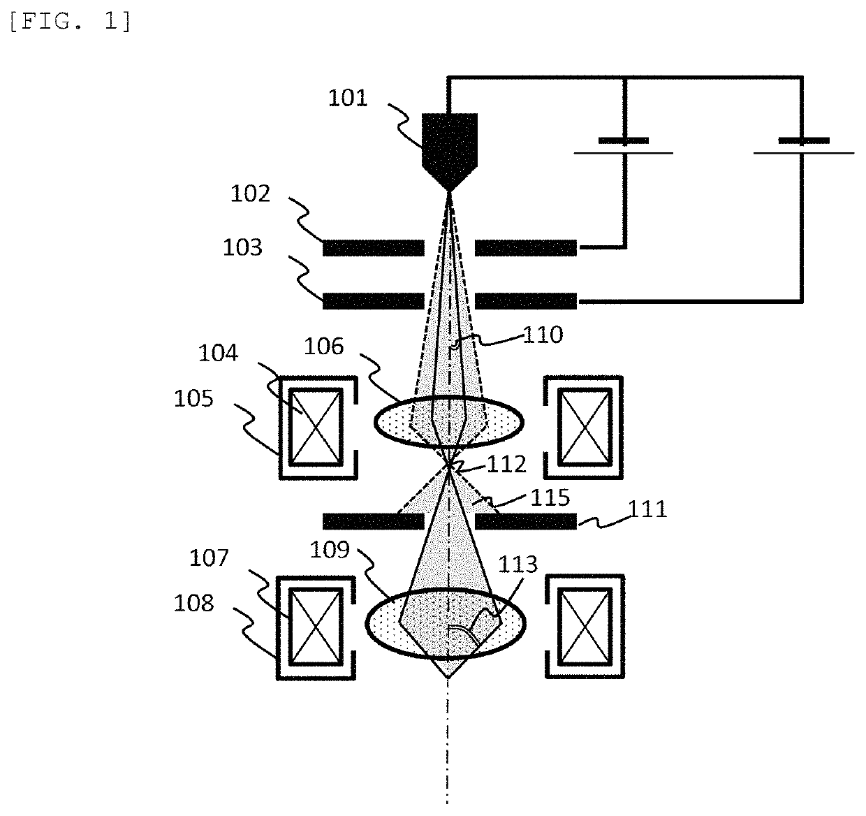
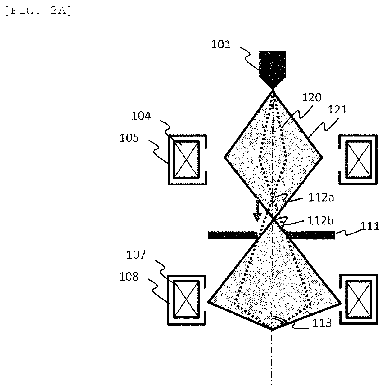
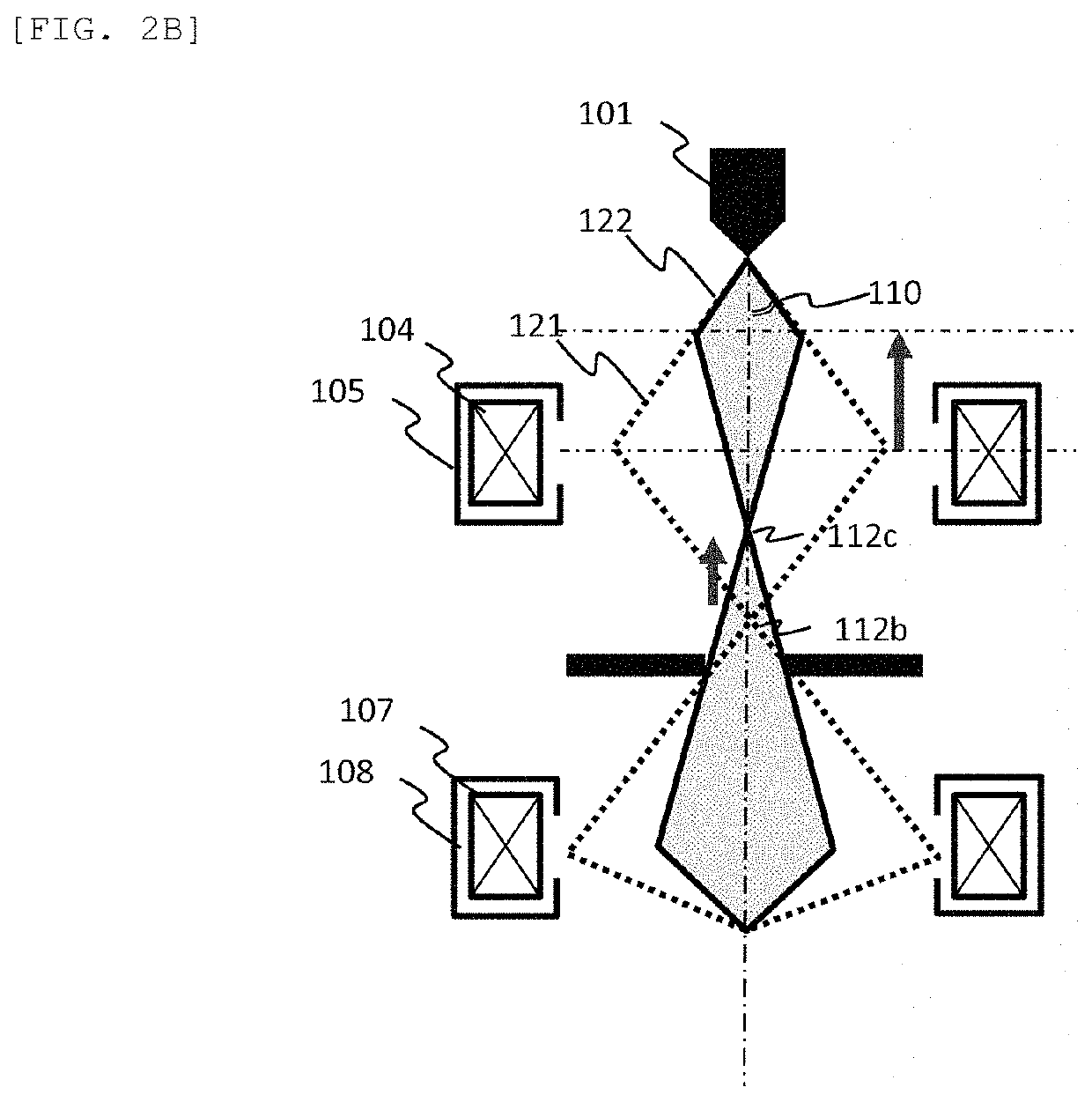
TECHNICAL FIELD[0001]The present invention relates to an electron gun used in an electron beam application device such as an electron microscope, or an electron beam application device including the electron gun.BACKGROUND ART[0002]A scanning electron microscope (SEM) is widely used for visualization of a fine structure. The SEM is used not only for an observation of a form of a material such as metal and an observation of a fine shape and form of a biological sample, but also for a dimensional inspection and defect inspection and the like of a semiconductor fine pattern. The SEM scans a measurement sample while irradiating the measurement sample with an electron beam, and detects signal electrons (secondary electrons and / or reflected electrons) emitted from the measurement sample to obtain a scanning image (SEM image).[0003]Image quality of the SEM image is mainly determined by two points: image roughness and image sharpness. The SEM converges the electron beam emitted from an elec...

Claims


Application Information

Patent Timeline
Patent Type & Authority Applications(United States)
IPC IPC(8): H01J37/063H01J37/141H01J37/244H01J37/248H01J37/28H01J37/295
CPCH01J37/295H01J37/244H01J37/141H01J37/248H01J37/063H01J37/28H01J37/07H01J2237/06375
Inventor MATSUNAGA, SOICHIROSOHDA, YASUNARIKATAGIRI, SOUICHISAKAKIBARA, MAKOTOKAWANO, HAJIMEDOI, TAKASHI
Owner HITACHI HIGH-TECH CORP
Learn More