Improved system for electron diffraction analysis

a technology of electron diffraction and electron diffraction pattern, which is applied in the field of improving the sensitivity of electron diffraction pattern analysis, can solve the problems of affecting the detection of contrast of real interest, affecting the detection accuracy of real interest, and less effective flat-fielding procedure, so as to reduce the angular variation in intensity, minimize the dynamic range, and improve the effect of detection accuracy

Active Publication Date: 2020-08-27
OXFORD INSTR NANOTECH TOOLS
View PDF0 Cites 1 Cited by
  • Summary
  • Abstract
  • Description
  • Claims
  • Application Information

AI Technical Summary

Benefits of technology

[0060]The minimizing of the dynamic range may comprise reducing to the smallest degree possible, or reducing to less than a predetermined threshold, the dynamic range of the image. Such conditions typically correspond to minimized angular variation in intensity of electrons imaged from the calibration sample. The optimizing the process so as to identify conditions that result in the dynamic range being minimized may involve adjusting the conditions, such as the geometry as noted above, until a minimum or a suitably low dynamic range is found, or it may be performed by adjusting the conditions according to a known relationship with or effect on the dynamic range. For example, an increased distance between the detector and the specimen, a reduced tilt angle between the beam axis and the specimen, or the normal vector of the specimen surface on which the beam impinges, would be understood to affect the dynamic range in a predictable manner.
[0061]It is possible to improve the accuracy of the removal of the gain variation pattern by way of performing the “calibration step” multiple times. Thus in some embodiments, the method further comprises: repeating at least once, the steps of obtaining, according to a respective further set of microscope conditions, a calibration image, and obtaining therefrom a gain variation image comprising a plurality of pixels, each having a value representing a calculated value for a relative detector device gain value for a corresponding pixel of the calibration image, so as to obtain at least one further gain variation image: obtaining more than one gain variation image may be beneficial in a number of applications. For instance, because of the above noted relationship between the relative pixel gain and incident electron beam energy for the beam impinging upon the specimen, it is preferable that the energy of the electron beam using which the calibration image, and therefore the gain variation image, are obtained is similar to, or more preferably the same as, the incident beam energy that is to be used for obtaining the target image. In light of this, obtaining multiple calibration images using different beam energies may be advantageous since doing so would allow an appropriate calibration image, and corresponding gain variation image derived therefrom to be selected in accordance with the beam energy comprised by the second set of microscope conditions with which the target image is obtained. Thus, in some embodiments where the obtaining of the calibration image and gain variation image are repeated, each of the first and further sets of microscope conditions comprises a different beam energy. In such cases, the gain variation-corrected image may be obtained by removing from the target image pixel values the contribution to the pixel values of the relative detector device gain in accordance with the corresponding pixel values of one of the first and further gain variation images that is selected in accordance with the microscope conditions under which the selected corresponding calibration image was obtained. In particular, the selection may be made based upon a similarity or calculated comparison between the second set of microscope conditions and the set of microscope conditions corresponding to the one of the first and further gain variation images that is selected. In particular, the comparison is preferably assessed based on the beam energy of the aforementioned sets of microscope conditions.
[0062]In some embodiments, the method further comprises combining the first and at least one further gain variation images to obtain a combined gain variation image, wherein the gain variation-corrected image is obtained in accordance with the combined gain variation image. In this way, the first, and one or more, gain variation images may be used in combination to achieve a combined gain variation image that may more accurately represent the relative detector device gain values effecting images acquired by that detector device. The combining may be performed, for example, by image averaging. For instance, for each pixel of the first gain variation image, the pixel value may be combined by way of an average, such as a mean or weighted mean, with the value of the corresponding pixel in each of the at least one further gain variation images.

Problems solved by technology

However, when analysing particles rather than a flat sample, Small and Michael note that the angular distribution of the diffuse background depends on the local geometry of incidence on the particle and the greater the difference between the angular distribution of the background and particle EBSD pattern images, the less effective the flat-fielding procedure and the lower the quality of the corrected EBSD pattern.
Dingley et al. point out that dynamic background correction has a few drawbacks over the conventional “static background correction” approach because any defects in the phosphor screen (such as scratches or pores, or the small-scale granular texture inherent to phosphor screens) are not removed using the dynamic approach whereas the static background approach is very effective at removing them.
However, due to the method of read-out of CMOS image pixels, the CMOS sensor image often exhibits fixed pattern artefacts such as line noise and the combination of a patterned fibre optic and a CMOS image sensor typically results in a pixel gain variation, G(J), that shows high contrast at high spatial frequencies and thus interferes with detection of the contrast of real interest, D(J).
As discussed above, the static background approach can be used to correct for these pixel gain variations but requires an appropriate reference specimen and careful control of acquisition of the reference image which is inconvenient and requires skill.
Furthermore, if the specimen has phases with different atomic number, then a single static background reference cannot be used for correcting patterns from all over the specimen.
Therefore, when dynamic background correction is used, the high-frequency detail due to pixel gain variations interferes with the high-frequency detail that defines the diffraction contrast so neither conventional static or dynamic background correction provides an effective solution when there is substantial variation in effective pixel gain.

Method used


Image

  • Improved system for electron diffraction analysis
  • Improved system for electron diffraction analysis
  • Improved system for electron diffraction analysis

Examples


Embodiment Construction

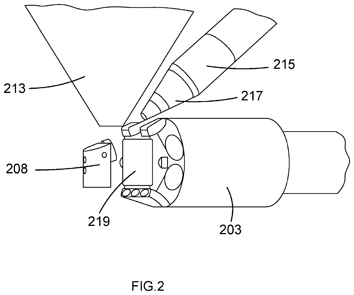
[0092]When an image is recorded from scattered electrons using a typical geometry as shown in FIG. 2 with the specimen tilted 70 degrees so that the incident beam makes an angle of 20 degrees with the surface, a typical camera system that uses a phosphor, conventional optical lenses and a charge coupled device (CCD) image sensor will record an image resembling that shown in FIG. 5.

[0093]The image intensity varies considerably across the field of view and the weak Kikuchi diffraction lines are seen as a modulation of the background due to diffusely scattered electrons. This is apparent in the intensity profile in FIG. 6 that shows intensity values along a line across the middle of the image where the diffraction contrast is seen as a high frequency ripple on top of a slowly varying background. If this profile is smoothed using a digital convolution filter where the support of the filter is much wider than the period of oscillation of the diffraction detail and typically more than 10%...


PUM


Abstract

A method and system for processing a diffraction pattern image obtained in an electron microscope are disclosed. The method comprises, according to a first set of microscope conditions, causing an electron beam to impinge upon a calibration specimen so as to cause resulting electrons to be emitted therefrom and monitoring the resulting electrons using a detector device so as to obtain a calibration image comprising a plurality of pixels having values, the first set of microscope conditions being configured such that the calibration image includes substantially no electron diffraction pattern; obtaining, from the calibration image, a gain variation image comprising a plurality of pixels, each having a value representing relative detector device gain for a corresponding pixel of the calibration image; according to a second set of microscope conditions, causing an electron beam to impinge upon a target specimen so as to cause resulting electrons to be emitted therefrom and monitoring the resulting electrons using the detector device so as to obtain a target image comprising a plurality of pixels having values, the second set of microscope conditions being configured such that the target image includes an electron diffraction pattern; and for each pixel of the target image, removing from the pixel value, in accordance with the value of the corresponding pixel of the gain variation image, the contribution to the pixel value of the relative detector device gain, so as to obtain a gain variation-corrected image.

Description

FIELD OF INVENTION[0001]The present invention relates to a system and method for improving the sensitivity of electron diffraction pattern analysis in an electron microscope and in particular analysis of Kikuchi patterns.BACKGROUND TO THE INVENTION[0002]FIG. 1 is a schematic showing some parts of a system that are employed in a scanning electron microscope (SEM) for exploring the surface of a specimen. The electron beam, with typical energy between 5 keV and 30 keV, is produced inside an evacuated chamber and usually focussed with a combination of magnetic lenses within the “SEM column”101. When the focussed beam 105 strikes a specimen 107, some electrons are scattered back from the specimen (backscattered electrons or BSE). For the last 30 years, systems have been commercially available for detecting the Kikuchi band patterns that are caused by diffraction of the emerging backscattered electrons, sometimes called “electron backscatter diffraction patterns” or EBSD patterns. These s...

Claims


Application Information

Patent Timeline
Patent Type & Authority Applications(United States)
IPC IPC(8): H01J37/244H01J37/22H01J37/26H01J37/295
CPCH01J37/244H01J37/295H01J2237/226H01J37/222H01J37/265H01J2237/24475H01J2237/221
Inventor STATHAM, PETERBEWICK, ANGUS
Owner OXFORD INSTR NANOTECH TOOLS
Why Eureka
Try Eureka