
Photoelectric conversion device and imaging apparatus

Active Publication Date: 2020-09-17
SONY CORP +1
View PDF0 Cites 0 Cited by
  • Summary
  • Abstract
  • Description
  • Claims
  • Application Information

AI Technical Summary

Benefits of technology

This patent is about a new device that converts light into electricity using an organic semiconductor material. The device has a layer where the semiconductor material forms a crystal structure. The patent describes how the ratio between different crystals can be controlled, which helps to improve the function of the device. This can reduce defects and improve the efficiency with which light is converted to electricity. The patent also describes a method for controlling the mixture of the semiconductor material in the device, which can further enhance its performance. Overall, this patent presents a way to create better quality photoelectric conversion devices using organic materials.

Problems solved by technology

However, the organic photoelectric conversion device has a problem that sufficient quantum efficiency cannot be obtained due to a low conductive characteristic of an organic semiconductor.
In addition, the organic imaging device has a problem that an electric output signal is easily delayed with respect to entering light.

Method used


Image

  • Photoelectric conversion device and imaging apparatus
  • Photoelectric conversion device and imaging apparatus
  • Photoelectric conversion device and imaging apparatus

Examples


first embodiment

1. FIRST EMBODIMENT

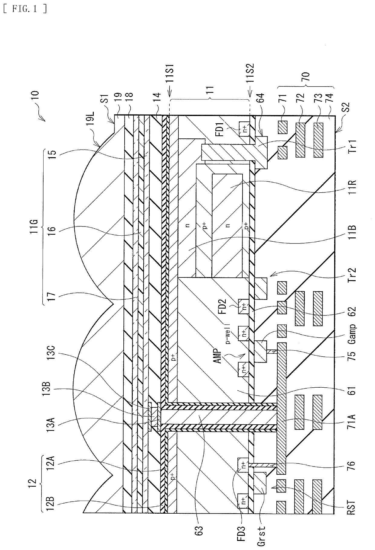
[0066]FIG. 1 Illustrates a cross-sectional configuration of a photoelectric conversion device (photoelectric conversion device 10A) according to a first embodiment of the present disclosure. The photoelectric conversion device 10A is, for example, an imaging device that configures a single pixel (unit pixel P) in an imaging apparatus (imaging apparatus 1) such as a CCD (Charge Coupled Device) image sensor or a CMOS (Complementary Metal Oxide Semiconductor) image sensor of a back illumination type (back light receiving type) (see FIG. 19). The photoelectric conversion device 10A is of a so-called vertical spectroscopic type in which a single organic photoelectric conversion section 11G and two inorganic photoelectric conversion sections 11B and 11R are stacked in a vertical direction. The organic photoelectric conversion section 11G and the two inorganic photoelectric conversion sections 11B and 11R selectively detect light in different wavelength ranges to perform...

second embodiment

2. SECOND EMBODIMENT

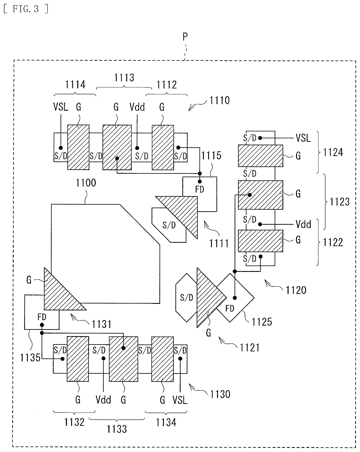
[0145]FIG. 9 illustrates a cross-sectional configuration of a photoelectric conversion device (photoelectric conversion device 10B) of a second embodiment of the present disclosure. FIG. 10 is an equivalent circuit diagram of the photoelectric conversion device 10B illustrated in FIG. 9. FIG. 11 schematically shows arrangement of the lower electrode 21 and transistors configuring the control unit of the photoelectric conversion device 10B illustrated in FIG. 9. As with the photoelectric conversion device 10A, the photoelectric conversion device 10B is an imaging device that configures one pixel (unit pixel P) in an imaging apparatus (imaging apparatus 1) such as a CCD image sensor or a CMOS image sensor of a back illumination type (back surface light receiving type), for example. The photoelectric conversion device 10B is of a so-called vertical spectroscopic type in which a single organic photoelectric conversion section 20 and two inorganic photoelectric conver...

application examples

3. APPLICATION EXAMPLES

Application Example 1

[0210]FIG. 19 illustrates, for example, an overall configuration of the imaging apparatus 1 in which the photoelectric conversion device 10A (or the photoelectric conversion device 10B) described in the embodiment described above is used for each pixel. This imaging apparatus 1 is a CMOS image sensor. The imaging apparatus 1 includes a pixel unit 1a as an imaging region on the semiconductor substrate 11. The imaging apparatus 1 also includes a peripheral circuit unit 130 in a surrounding region of the pixel unit 1a. The peripheral circuit unit 130 includes, for example, a row scanning unit 131, a horizontal selecting unit 133, a column scanning unit 134, and a system control unit 132.

[0211]The pixel unit 1a includes a plurality of unit pixels P (corresponding to the photoelectric conversion section 10, for example) two-dimensionally disposed in matrix, for example. In the unit pixel P, a pixel drive line Lread (specifically, a row select l...


PUM


Abstract

[Problem] Provided are a photoelectric conversion device and an imaging apparatus capable of improving quantum efficiency and a response speed.[Solving means] A first photoelectric conversion device according to one embodiment of the present disclosure includes a first electrode, a second electrode opposed to the first electrode, and a photoelectric conversion layer. The photoelectric conversion layer is provided between the first electrode and the second electrode and includes at least one type of one organic semiconductor material having crystallinity. Variation in a ratio between horizontally-oriented crystal and vertically-oriented crystal in the photoelectric conversion layer is three times or less between a case where film formation of the one organic semiconductor material is performed at a first temperature and a case where the film formation of the one organic semiconductor material is performed at a second temperature. The second temperature is higher than the first temperature.

Description

TECHNICAL FIELD[0001]The present disclosure relates to, for example, a photoelectric conversion device using an organic semiconductor material and an imaging apparatus including this.BACKGROUND ART[0002]In recent years, devices using organic thin films have been developed. One of such devices is an organic photoelectric conversion device. There has been proposed an organic thin-film solar cell, an organic imaging device, or the like using it. In the organic photoelectric conversion device, a bulk heterostructure in which a p-type organic semiconductor and an n-type organic semiconductor are mixed is employed to improve quantum efficiency (for example, see PTL 1). However, the organic photoelectric conversion device has a problem that sufficient quantum efficiency cannot be obtained due to a low conductive characteristic of an organic semiconductor. In addition, the organic imaging device has a problem that an electric output signal is easily delayed with respect to entering light.[0...

Claims


Application Information

Patent Timeline
IPC IPC(8): H01L27/30H01L51/00
CPCH01L51/0077H01L27/307H01L51/0074H01L51/0067H01L51/0046H01L27/146Y02E10/549C07D495/04A61B90/361A61B2090/309A61B2090/304C07D495/14C07D333/08H10K39/32H10K71/40H10K85/655H10K85/731H10K85/6576H10K85/6574H10K30/30H10K85/322H10K85/211H10K85/311H10K85/615H10K85/6572H10K30/81H10K30/86H10K30/85H10K85/30H10K85/654H10K85/631
Inventor KATO, YUINABA, YUTAKANNO, MASATOMOGI, HIDEAKIKIMIJIMA, MIKIMIYAJI, SAE
Owner SONY CORP
Learn More