Method for manufacturing semiconductor device

Active Publication Date: 2010-04-15
PANASONIC CORP
View PDF2 Cites 16 Cited by
  • Summary
  • Abstract
  • Description
  • Claims
  • Application Information

AI Technical Summary

Benefits of technology

[0022]Furthermore, a problem has also been found in that, depending on the material of the surface dielectric layer used for the electrostatic chuck, a large number of particles may adhere to the semiconductor wafer, thus lowering the production yield of the semiconductor device.
[0027]The present invention has been made in order to solve the above problems, and a main objective thereof is to, in a production method for a semiconductor device which performs a high-temperature ion implantation by using an electrostatic chuck, reduce occurrence of defects that are formed on an attracted face of a semiconductor wafer.Means for Solving the Problems
[0040]According to the present invention, even when a semiconductor wafer is attracted by using an electrostatic chuck which is heated to a high temperature of 400° C. or more, the presence of a protection film which is provided on the semiconductor wafer effectively reduces formation of defects on an attracted face of the semiconductor wafer.

Problems solved by technology

However, an ion implantation for silicon carbide semiconductor has a unique problem in that the ion implantation needs to be performed at a high temperature.
However, such an activation annealing alone will not suffice, and it is considered necessary to maintain the silicon carbide substrate at a high temperature of 400° C. or more even while the ion implantation is being performed (e.g., Patent Document 4, Non-Patent Document 1, Non-Patent Document 2).
Thus, the conventional method which fixes a semiconductor wafer onto a carbon susceptor via screwing has a problem of very low throughput and poor mass producibility.

Method used


Image

  • Method for manufacturing semiconductor device
  • Method for manufacturing semiconductor device
  • Method for manufacturing semiconductor device

Examples


first embodiment

[0095]First, a first embodiment of a production method for a semiconductor device according to the present invention will be described. In the present embodiment, an Si wafer is used as a semiconductor wafer.

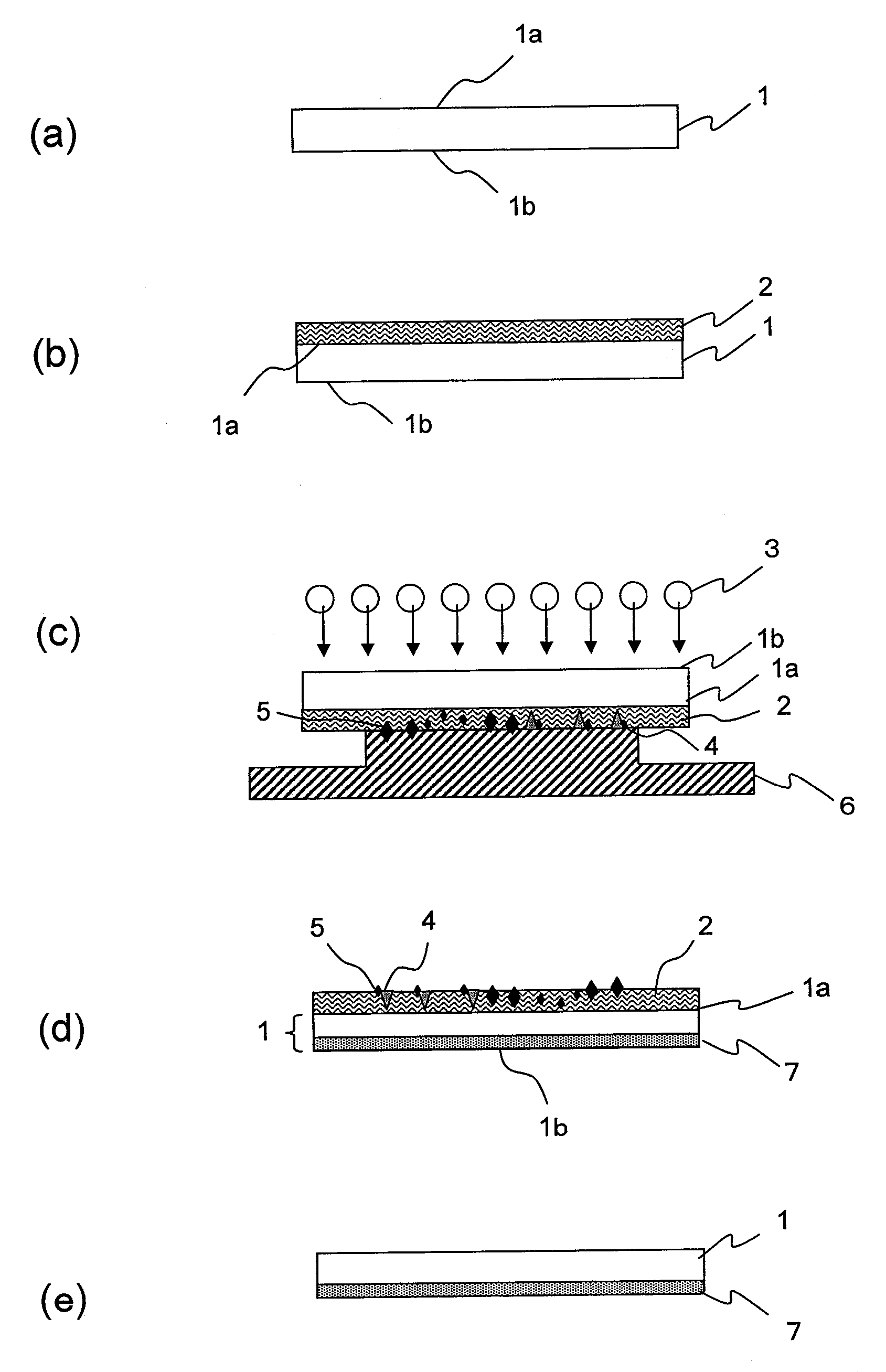
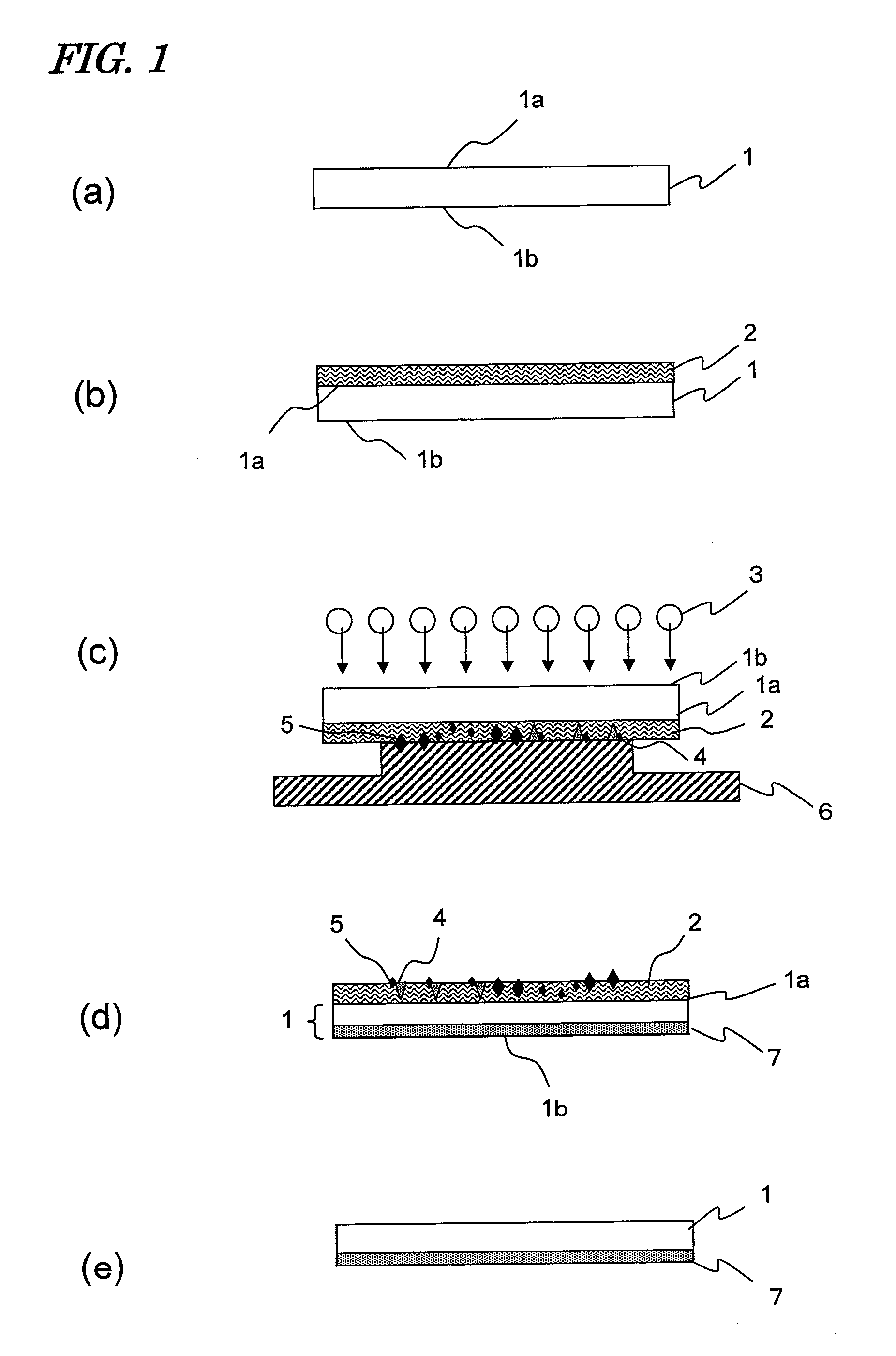
[0096]With reference to FIG. 1, a production method for a semiconductor device according to the present embodiment will be described. FIGS. 1(a) to (e) are cross-sectional views showing a flow of steps of the present embodiment.

[0097]First, as shown in FIG. 1(a), a plurality of semiconductor wafers 1 each having a first face (principal face) 1a and a second face (rear face) 1b were provided. Each of the semiconductor wafers 1 used herein was an n type Si wafer having a diameter of 3 inches, with a specific resistance of 10 to 20 Ω·cm. Thereafter, as shown in FIG. 1(b), a protection film 2 was formed on the first face 1a of the semiconductor wafer 1. Specifically, four semiconductor wafers 1 having four types of different protection films 2 deposited on the first face 1a thereof,...

second embodiment

[0125]Hereinafter, a second embodiment of a production method for a semiconductor device according to the present invention will be described. In the present embodiment, the attracting face of the electrostatic chuck is made of pyrolytic boron nitride (pBN). pBN is a material with a layered structure, and is a material whose hardness is significantly lower than that of AlN.

[0126]The temperature of the attracting face of the electrostatic chuck was set to 460° C., similarly to the first embodiment. In the present embodiment, the following seven different types of semiconductor wafers were provided.

[0127](E) an Si wafer lacking a protection film

[0128](F) an Si wafer with SiO2 (thickness 1 μm)

[0129](G) an SiC wafer lacking a protection film

[0130](H) an SiC wafer with SiO2 (thickness 1 μm)

[0131](I) an Si wafer with SiO2 ((thickness 0.1 μm)

[0132](J) an SiC wafer with SiO2 ((thickness 0.1 μm)

[0133](K) an SiC wafer with poly-Si (thickness 800 nm) / thermal oxide film (thickness 70 nm)

[0134]E...

third embodiment

[0150]Hereinafter, a third embodiment of a production method for a semiconductor device according to the present invention will be described. In the present embodiment, a vertical MISFET of silicon carbide semiconductor is produced.

[0151]First, FIG. 7 is referred to. FIGS. 7(a) to (h) are step-by-step cross-sectional views showing production steps of a vertical MISFET of silicon carbide semiconductor according to the present embodiment.

[0152]In the present embodiment, the chuck surface of the electrostatic chuck 6 is made of pBN, and the setting temperature of the electrostatic chuck 6 is 460° C.

[0153]First, as shown in FIG. 7(a), a semiconductor wafer 1 is provided in which a drift layer 102 of silicon carbide is epitaxially grown on a silicon carbide substrate 101. In the present specification, in the case where a semiconductor layer is formed on the surface of the semiconductor substrate, the entire body will be referred to as the “semiconductor wafer”. A first face 1a of the sem...


PUM


Abstract

On one face of a semiconductor wafer 1 having a first face (principal face) 1a and a second face (rear face) 1b, a protection film 2 is formed. When allowing the semiconductor wafer 1 to be attracted onto an attracting face of an electrostatic chuck 6 which is heated to 400° C. or more, the semiconductor wafer 1 is attracted onto the attracting face via the protection film 2. While heating the semiconductor wafer 1 to 400° C. or more, an ion implantation is performed for the face of the semiconductor wafer 1 on which the protection film 2 is not formed. Thereafter, the protection film 2 is removed from the semiconductor wafer 1.

Description

TECHNICAL FIELD[0001]The present invention relates to a production method for a semiconductor device which is performed by using an electrostatic chuck, and in particular to a production method for a semiconductor device which includes a step of attracting a semiconductor wafer with an electrostatic chuck that is heated to a high temperature of 400° C. or more.BACKGROUND ART[0002]A power device is a semiconductor element in which a large current flows, and is expected to have a high breakdown voltage and a low loss. Conventionally, power devices in which silicon (Si) semiconductor is used have been in the main stream. In recent years, however, power devices in which silicon carbide (SiC) semiconductor is used are drawing attention and are under development. A silicon carbide semiconductor has a breakdown field which is one digit higher than that of silicon, and therefore is able to maintain a reverse voltage even if the depletion layer of a PN junction or a Schottky junction is redu...

Claims


Application Information

Patent Timeline
IPC IPC(8): H01L21/265
CPCH01J2237/2001H01L29/0619H01L29/1608H01L29/7811H01L29/6606H01L29/66068H01L29/7802H01L29/45H01L29/0878
Inventor KUSUMOTO, OSAMUKUDOU, CHIAKITAKAHASHI, KUNIMASA
Owner PANASONIC CORP
Why Eureka
Try Eureka