Eureka AIR delivers breakthrough ideas for toughest innovation challenges, trusted by R&D personnel around the world.

Barrier layer for electroplating processes

Inactive Publication Date: 2005-02-10
APPLIED MATERIALS INC
View PDF21 Cites 1 Cited by
  • Summary
  • Abstract
  • Description
  • Claims
  • Application Information

AI Technical Summary

Benefits of technology

[0019] The invention generally provides a method for preparing a substrate prior to electroplating for forming void-less metal interconnects in sub-micron, high aspect ratio features on semiconductor substrates. The invention overcomes the problems presented by currently practiced barrier layers used in electroplating and reduces the formation of defective devices caused by unsatisfactory electroplating results. Generally, the invention provides a method for forming a high conductance (i.e., resistivity <<160μΩ-cm) barrier layer on which metal can be electro-chemically deposited to significantly reduce the defect formations formed during the electroplating process due to discontinuities in the seed layer.
[0020] One aspect of the invention provides a method for preparing a surface for electrochemical deposition comprising forming a high conductance barrier layer on the surface and depositing a seed layer over the barrier layer. Preferably, the high conductance barrier layer comprises a material selected from tungsten, tungsten nitride (WNx, where x≦3), titanium and titanium nitride, and / or combinations thereof. The high conductance barrier layer provides a surface on which metal can be electro-chemically deposited and therefore, significantly reduces the defect formations formed during the electroplating process due to discontinuities in the seed layer.

Problems solved by technology

Many traditional deposition processes have difficulty filling structures where the aspect ratio exceeds 4:1, and particularly where it exceeds 10:1 and is less than 0.25 μm wide.
Therefore, there is a great amount of ongoing effort being directed at the formation of void-free, sub-micron high aspect ratio features.
Despite the desirability of using copper for semiconductor device fabrication, choices of fabrication methods for depositing copper into very high aspect ratio features are limited because common chemical vapor deposition processes and physical vapor deposition processes have provided unsatisfactory results for forming voidless metallization of sub-micron high aspect ratio interconnect features.
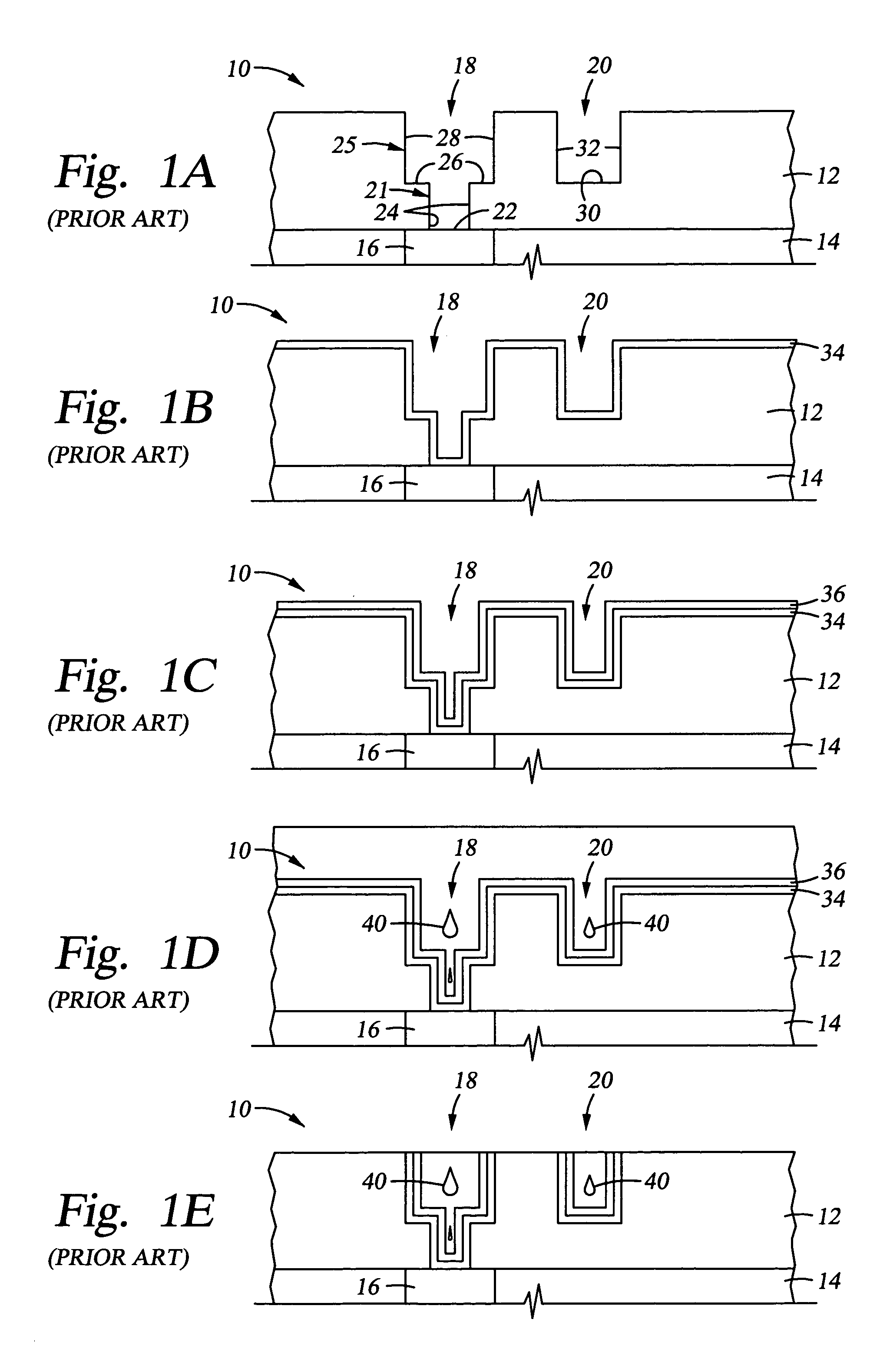
However, the electroplating metallization process presently practiced typically forms voids 40 in the interconnect features that may lead to defective devices or premature breakdown of the devices, as discussed in more detail below.
However, a number of obstacles impair consistent electroplating of copper onto substrates having sub-micron, high aspect ratio features.
Particularly with physical vapor deposition of a seed layer, it is very difficult to deposit a continuous, uniform seed layer within a high aspect ratio, sub-micron feature.
The seed layer tends to become discontinuous especially at the bottom surface of the feature because it is difficult to deposit through the narrow (i.e., sub-micron) aperture width of the feature.
The discontinuities in the seed layer prevent proper electroplating of the metal onto the seed layer, resulting in defective devices on the processed substrate.
Second, discontinuities in the metal seed layer also cause void formations in high aspect ratio interconnect features.
The void changes the material and operating characteristics of the interconnect feature and may cause improper operation and premature breakdown of the device.

Method used

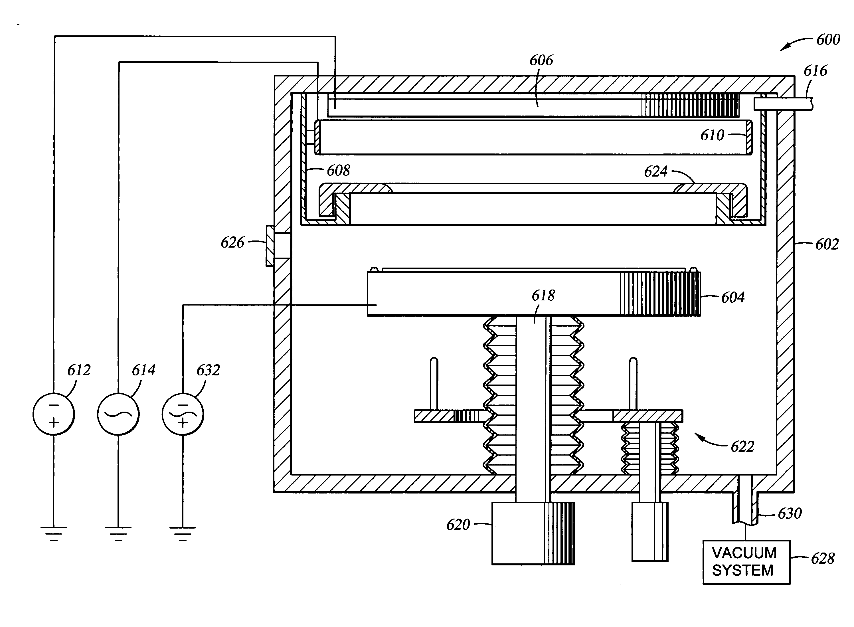
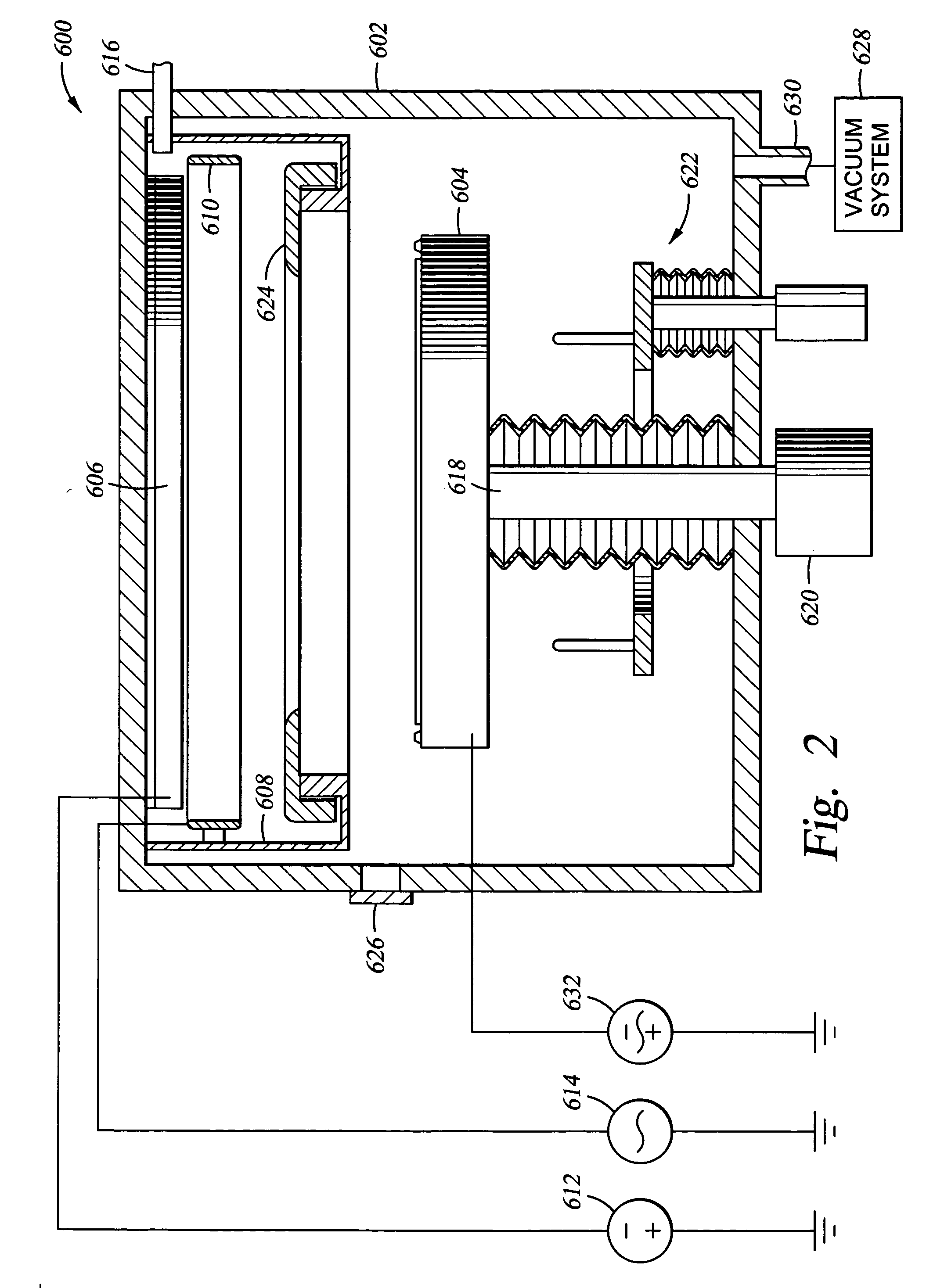

Image

  • Barrier layer for electroplating processes
  • Barrier layer for electroplating processes
  • Barrier layer for electroplating processes

Examples


Embodiment Construction

[0031] The present invention provides methods for improving the electroplating fill of high aspect ratio, sub-micron interconnect features. Although the invention is described using a dual damascene structure on a substrate, the invention contemplates applications in other interconnect features and other integrated circuit features (i.e., lines, vias, contacts, plugs, etc.) that require filling the features formed on a substrate with a metal. Also, although the invention is described using copper as the electroplated metal for metallization of the feature, the invention is applicable to other metals that can be electroplated onto a substrate.

[0032] Generally, a continuous metal seed layer is essential for conducting an electrical current to the surfaces to be plated by the electroplating process. Typically, the seed layer is deposited using PVD techniques, which has not provided satisfactory results for forming a uniform, continuous seed layer at the bottom of high aspect ratio, su...


PUM

PropertyMeasurementUnit
Temperatureaaaaaaaaaa

Abstract

The invention generally provides a method for preparing a surface for electrochemical deposition comprising forming a high conductance barrier layer on the surface and depositing a seed layer over the high conductance barrier layer. Another aspect of the invention provides a method for filling a structure on a substrate, comprising depositing a high conductance barrier layer on one or more surfaces of the structure, depositing a seed layer over the barrier layer, and electrochemically depositing a metal to fill the structure.

Description

CROSS-REFERENCE TO RELATED APPLICATIONS [0001] This application is a continuation of co-pending U.S. patent application Ser. No. 10 / 016,255, filed Dec. 10, 2001, which is a continuation of U.S. patent application Ser. No. 09 / 375,167, filed Aug. 16, 1999, now U.S. Pat. No. 6,328,871. The aforementioned related patent application is herein incorporated by reference.BACKGROUND OF THE INVENTION [0002] 1. Field of the Invention [0003] The present invention generally relates to electrochemical deposition or electroplating a metal onto a substrate. More particularly, the present invention relates to methods of forming a barrier layer and a seed layer prior to filling the structures formed on a substrate using an electroplating process. [0004] 2. Description of the Related Art [0005] Copper has become a choice metal for filling sub-micron, high aspect ratio interconnect features on substrates as circuit densities increase for the next generation of ultra large scale integration because copp...

Claims


Application Information

Patent Timeline
IPC IPC(8): C25D3/00C25D7/12C25D5/34H01L21/28H01L21/288H01L21/3205H01L21/768H01L23/52H01L23/522
CPCH01L21/2885H01L21/76843H01L21/76877H01L21/76864H01L21/76873H01L21/76846C25D3/00
Inventor DING, PEIJUNCHIANG, TONYYAO, TSE-YONGCHIN, BARRY
Owner APPLIED MATERIALS INC
Why Eureka
Eureka Blog
Learn More