Thin-Film Filter, Thin-Film Filter Substrate, Method of Manufacturing the Thin-Film Filter, Method of Manufacturing the Thin-Film Filter Substrate, MEMS Microphone and Method of Manufacturing the MEMS Microphone

Active Publication Date: 2020-09-17
SAE MAGNETICS (HK) LTD
View PDF0 Cites 1 Cited by
  • Summary
  • Abstract
  • Description
  • Claims
  • Application Information

AI Technical Summary

Benefits of technology

The patent text discusses the issue of punched resin films used as filters. These films have holes that allow air to flow through them, but the air stream can damage the edges of the holes, making the film less durable. The technical effect of this patent is to increase the durability of punched resin films by improving their ability to resist damage from air flow.

Problems solved by technology

However, for example, when the punching processing is performed with laser, a part, which is etched by laser irradiation, becomes debris (pieces), the debris are likely to adhere the inside of the holes of the punched resin films.
Further, the size of each hole becomes uneven caused by adhesion of the debris.
Therefore, the punched resin films, which the punching processing is performed with laser, are not able to be used as a filter.
Therefore, the punched resin films, which the punching processing is performed by wet etching, have low durability.

Method used


Image

  • Thin-Film Filter, Thin-Film Filter Substrate, Method of Manufacturing the Thin-Film Filter, Method of Manufacturing the Thin-Film Filter Substrate, MEMS Microphone and Method of Manufacturing the MEMS Microphone
  • Thin-Film Filter, Thin-Film Filter Substrate, Method of Manufacturing the Thin-Film Filter, Method of Manufacturing the Thin-Film Filter Substrate, MEMS Microphone and Method of Manufacturing the MEMS Microphone
  • Thin-Film Filter, Thin-Film Filter Substrate, Method of Manufacturing the Thin-Film Filter, Method of Manufacturing the Thin-Film Filter Substrate, MEMS Microphone and Method of Manufacturing the MEMS Microphone

Examples


modified example 1

[0100]Next, the thin-film filter 32, according to a modified example 1, is explained with reference to FIG. 12, FIG. 13. FIG. 12 is a plan view showing a principal part of the thin-film filter 32 according to the modified example 1. FIG. 13 is a plan view showing a part, including representative through holes 15a, 15b, 15c, 15d, of the thin-film filter 32.

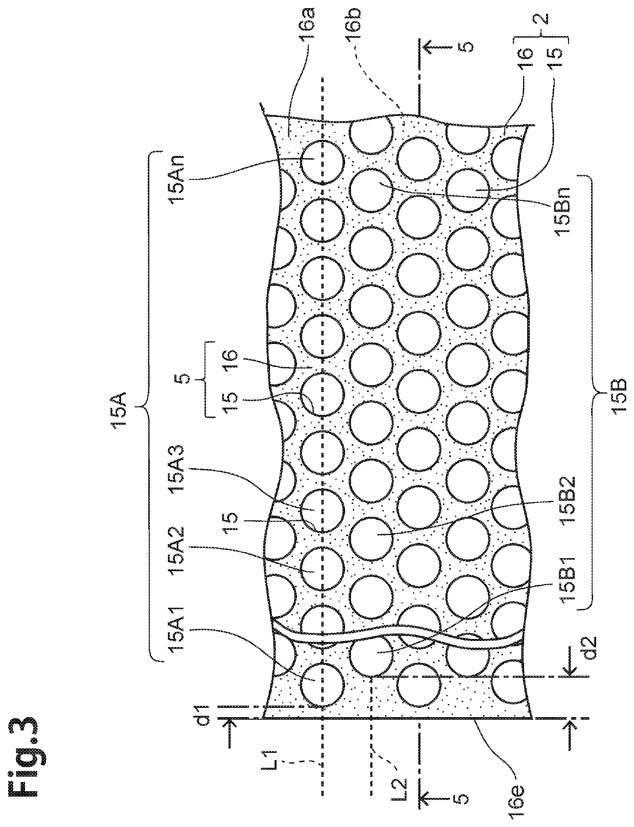
[0101]The thin-film filter 32 is different in that it has the first through hole-group 15A though, and it does not have the second through hole-group 15B, as compared with the thin-film filter 2. Because the thin-film filter 32 does not have the second through hole-group 15B, a plurality of the first lines L1 are arranged. Further, the first through hole 15A1, through holes 15A2, 15A3 . . . 15An, included in the each first line L1, are arranged at a constant interval in a straight line along with the direction intersecting vertically to the peripheral end part 16e. Furthermore, a plurality of first through holes 15A1, included in t...

modified example 2

[0105]Next, the thin-film filter 34, according to a modified example 2, is explained with reference to FIG. 14, FIG. 15, FIG. 16. FIG. 14 is a plan view, with enlargement, of the principal part of the thin-film filter 34 according to the modified example 2. FIG. 15 is a plan view, with more enlargement, of the principal part of the thin-film filter 34. FIG. 16 is a perspective view showing a sectional surface corresponding to the line 16-16 in FIG. 15.

[0106]The thin-film filter 34 is different in that it has a thin-film part 36 instead of the thin-film part 16, and the through holes 35 are formed instead of the through holes 15, as compared with the thin-film filter 2. The thin-film part 36 is different in that the through holes 35 are formed, as compared with the thin-film part 16.

[0107]The above-described through holes 15 are formed in circular shape in a plan view though, the through holes 35 are formed in a regular hexagon in a plan view. The thin-film filter 34 has a first thro...

modified example 3

[0111]Next, the thin-film filter substrate 30, according to a modified example 3, is explained with reference to FIG. 17. FIG. 17(a) is a plan view of a principal part of the thin-film filter substrate 30 according to the modified example 3. FIG. 17(b) is a perspective view showing the thin-film filter 2A, included in the thin-film filter substrate 30 and a reel member 199.

[0112]The thin-film filter substrate 30 has a filter panel 1A, as a base substrate, a thin-film filter 2A and the peeling-off adhesive layer 3.

[0113]The filter panel 1A is made of glass, and it is formed in a rectangular shape. The peeling-off adhesive layer 3 is formed on the base surface, being one side surface, of the filter panel 1A, and the thin-film filter 2A is formed on the peeling-off adhesive layer 3.

[0114]The thin-film filter 2A is different in its shape from the thin-film filter 2. The thin-film filter 2 is formed in a circular shape in accordance with the silicon wafer 1 though, the thin-film filter 2...


PUM


Abstract

A thin-film filter includes thin-film part having a film surface and a rear film surface arranged a rear side of the film surface, a plurality of through holes being formed to penetrate the thin-film part from the film surface to the rear film surface, and stripes-formed inner wall surfaces. The stripes-formed inner wall surfaces include stripe-like parts formed along with an intersecting direction intersecting the film surface. The stripes-formed inner wall surfaces are formed inside the respective through holes.

Description

CROSS REFERENCE TO RELATED APPLICATIONS[0001]The present application claims the benefit of Japanese Patent Application No. 2019-048174 filed on Mar. 15, 2019, the contents of which are incorporated herein by reference in their entirety.BACKGROUNDField of the Invention[0002]The present invention relates to a thin-film filter, being used for prevention of entry of particles, water or the like, a thin-film filter substrate having the thin-film filter, a method of manufacturing the thin-film filter, a method of manufacturing the thin-film filter substrate, a MEMS microphone having the thin-film filter and a Method of manufacturing the MEMS microphone.Related Background Art[0003]A filter is conventionally used for prevention of entry, to the inside, of micro things such as particles, cells or the like and water. Concerning such a filter, for example, a polymer film, which micro perforations are formed, is disclosed in patent document 1 (JP2015-199069). In case of the polymer film, diamet...

Claims


Application Information

Patent Timeline
IPC IPC(8): H04R19/04B81B7/00B81C1/00H04R31/00H04R1/08B01D39/16
CPCH04R19/04B81C2201/0194H04R2201/003B81C1/00333H04R31/00B01D39/1692B81B2201/0257H04R1/086B81B7/0058B01D2239/10H04R19/005B81B7/02B32B17/066B32B9/00B32B9/046B32B5/18B32B7/12B32B27/281B32B27/34B32B27/065B32B3/266B32B37/00B32B38/10B32B15/08B32B15/088H04R2231/00B32B2266/0271B32B2266/0214B01D2239/0654B81B2203/0127B81C1/00158B81B2207/012
Inventor TAKE, HIROSHIYOSHIDA, MAKOTOBINARAO, ANTHONY REYMUND MELADHENG, CHENG BU
Owner SAE MAGNETICS (HK) LTD
Why Eureka
Try Eureka