

Detection apparatus, detection substrate, and detection method
- Summary
- Abstract
- Description
- Claims
- Application Information
AI Technical Summary
Benefits of technology
Problems solved by technology
Method used
Image

Examples
embodiments
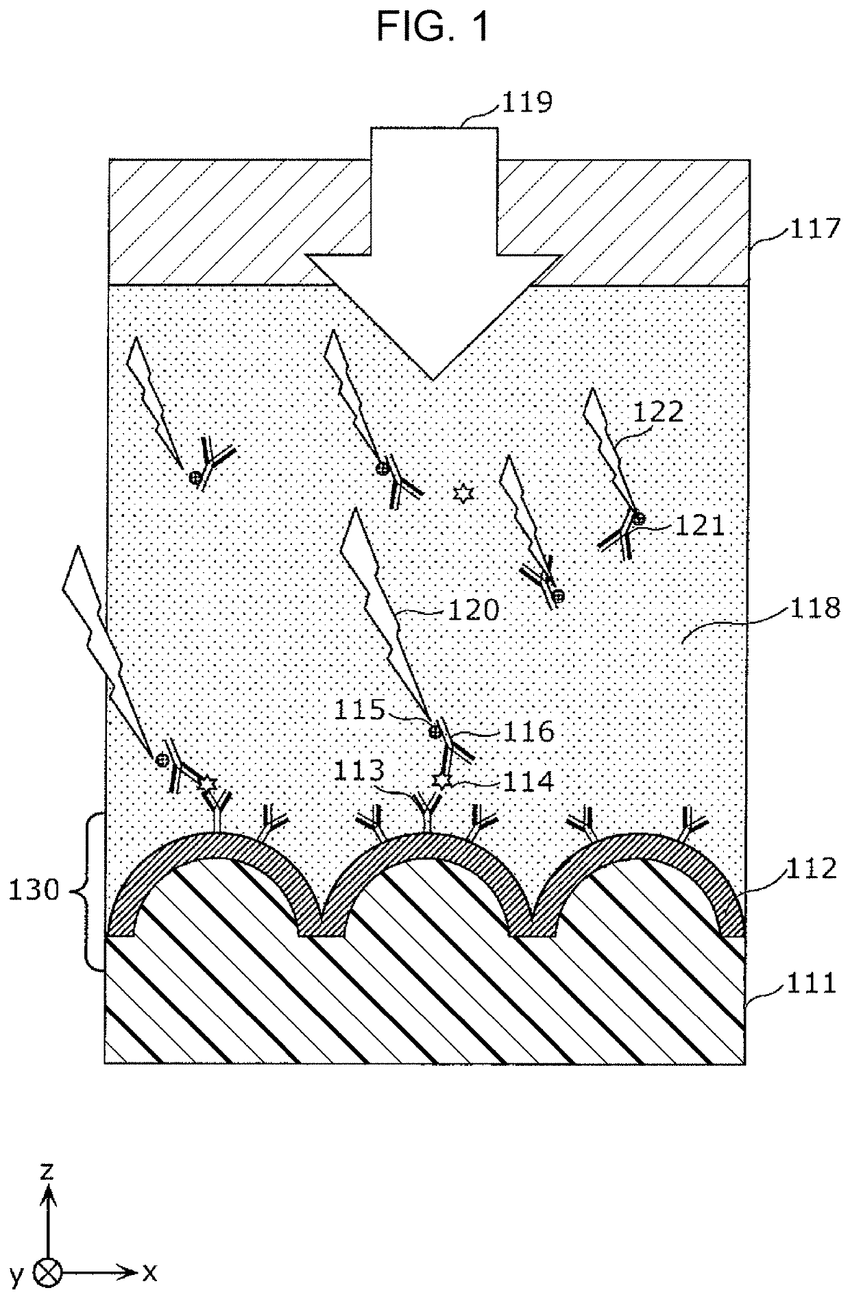
[0054]Hereinafter, embodiments will be specifically described with reference to the drawings.
[0055]Note that the embodiments described below each indicate a general or specific example. The numerical values, shapes, materials, constituent elements, arranged positions and connection forms of the constituent elements, steps, the order of the steps, and the like indicated in the following embodiments are each presented as an example and do not intend to limit the claims. Among the constituent elements in the following embodiments, constituent elements that are not described in an independent claim indicating a most generic concept are described as selective constituent elements. Each of the drawings is not necessarily strictly illustrated. In the drawings, constituents substantially identical to each other are given identical signs, and duplicate description thereof will be omitted or simplified.
Configuration of Detection Apparatus
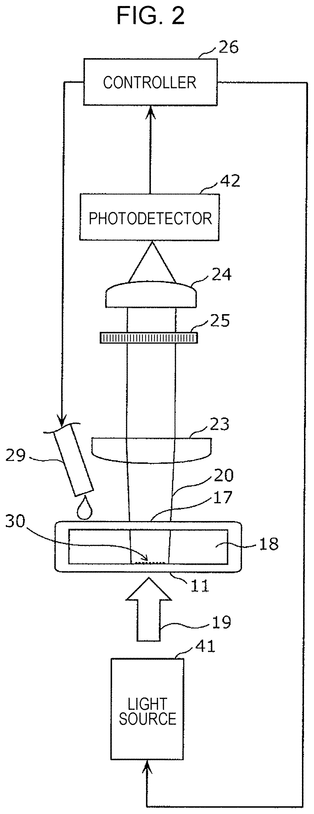
[0056]FIG. 2 is a block diagram of a detection apparatu...
example
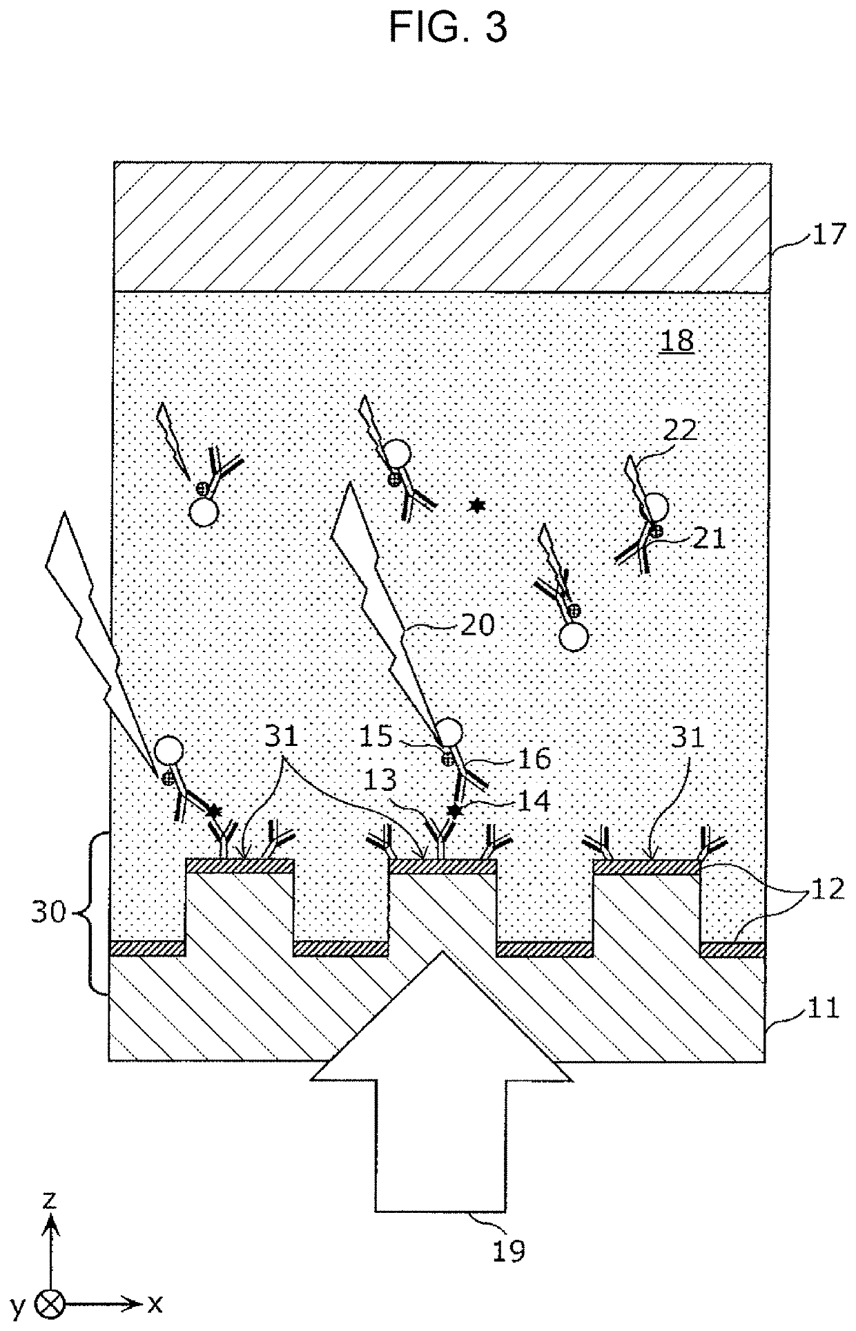
[0091]A result of simulation of the metal nanostructure will be described as an example of the present embodiment with reference to FIG. 7 to FIG. 10. FIG. 7 is a sectional view of a metal nanostructure according to an example.
[0092]In the simulation model of the present example, an olefin film was used as the substrate 11. On the olefin film, linear projections in which line width=100 nm, line height=200 nm, and line interval (pitch)=200 nm were formed. A metal nanostructure was formed on the substrate 11 by depositing silver, as the metal film 12, of a thickness of 175 nm. As a result, in the metal nanostructure, the linear light transmissive portions 32 with a width of Z=175 to 200 nm were formed on side surfaces (yz faces) of the linear projections.
[0093]The gold colloid 27 is positioned away from the metal film 12 by approximately 15 nm when the gold colloid is immobilized on the metal film 12 via a detection object. Therefore, in this simulation model, gold colloid was dispose...
PUM
 Abstract
Description
Claims
Application Information