Image sensors, methods, and pixels with floating diffusion and gate for charge storage

Inactive Publication Date: 2020-11-05
KRYMSKI ALEXANDER
View PDF0 Cites 1 Cited by
  • Summary
  • Abstract
  • Description
  • Claims
  • Application Information

AI Technical Summary

Benefits of technology

[0004]Various embodiments disclosed herein provide improvements for storing and transferring charge within pixels of an image sensor, so as to avoid a loss of charge and to facilitate the transfer of charge to provi

Problems solved by technology

This causes an exposure time skew, which can be observed in pictures of

Method used


Image

  • Image sensors, methods, and pixels with floating diffusion and gate for charge storage
  • Image sensors, methods, and pixels with floating diffusion and gate for charge storage
  • Image sensors, methods, and pixels with floating diffusion and gate for charge storage

Examples


Embodiment Construction

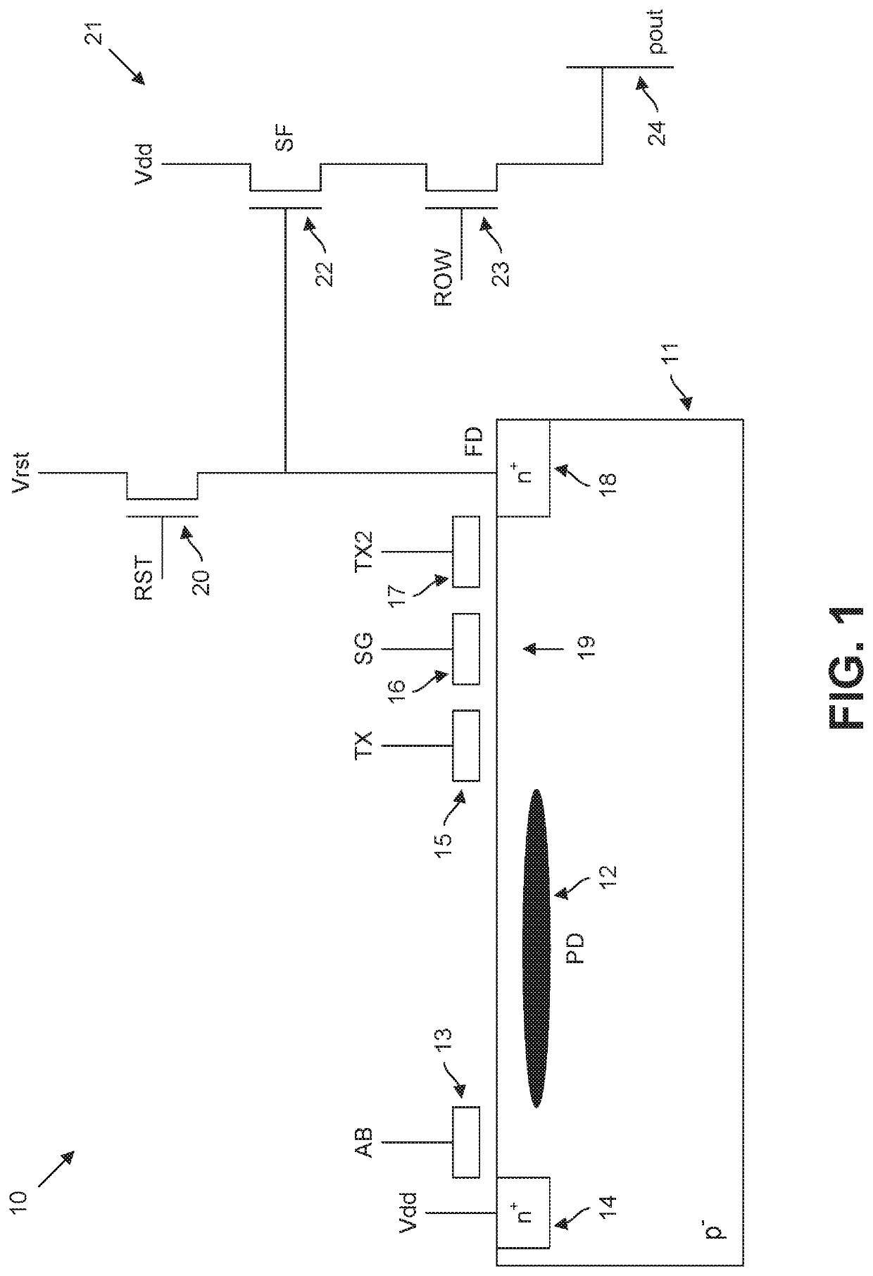
[0022]Various embodiments disclosed herein provide improvements for storing and transferring charge within pixels of an image sensor, so as to avoid a loss of charge and to facilitate the transfer of charge to provide accurate reads-out from the pixels. Also, various embodiments disclosed herein allow for a reduction in parasitic capacitance in pixels of an image sensor, so as to allow for a reduction in the size of the pixels.

[0023]FIG. 1 illustrates a pixel 10 in accordance with an embodiment of the present invention. The pixel 10 includes a substrate 11, a photodiode (PD) 12, an anti-blooming gate 13, a drain diffusion 14, a first transfer gate 15, a storage gate 16, a second transfer gate 17, a floating diffusion (FD) 18, a reset transistor 20, and a readout circuit 21. The readout circuit 21 includes a source follower transistor (SF) 22 and a read select transistor 23. The readout circuit 21 is connected to a readout line 24 for outputting signals from the pixel 10. The reset t...


PUM


Abstract

A pixel includes a photodiode, a first transfer gate, a second transfer gate, and a floating diffusion. The pixel may include a storage gate, and the first transfer gate may be controllable to transfer charge from the photodiode to an area under the storage gate. The storage gate is controllable to store the charge in the area under the storage gate and to transfer the charge from the area under the storage gate. The first transfer gate may be controllable among a first biasing condition in which charge is transferable to an area under the first transfer gate, a second biasing condition in which the charge is storable in the area under the first transfer gate, and a third biasing condition in which the charge is transferable out of the area under the first transfer gate. The second transfer gate is controllable to transfer charge to the floating diffusion.

Description

FIELD[0001]Embodiments of the present invention relate generally to image sensors, pixels, methods of using image sensors and pixels, and methods of manufacturing image sensors and pixels.BACKGROUND[0002]Image sensors have found wide application in consumer and industrial electronics, and have enabled an explosion in the number of digital cameras and digital video devices used for work and entertainment. An image sensor typically includes a pixel array with pixels that are arranged in rows and columns. Each pixel typically includes a light sensitive element, such as a photodiode, or the like, to sample light intensity of a corresponding portion of a scene being imaged, and each pixel is typically configured to produce an analog pixel signal based on the sampled light intensity.[0003]In some image sensors, there are different start and / or end times for the accumulation of charge in each row of pixels in the pixel array. This causes an exposure time skew, which can be observed in pict...

Claims


Application Information

Patent Timeline
IPC IPC(8): H01L27/146H04N5/378H04N5/3745
CPCH04N5/378H04N5/353H01L27/14689H04N5/37452H01L27/14643H01L27/14616H01L27/14614H01L27/14654H01L27/14612H04N25/771H04N25/75H04N25/53
Inventor KRYMSKI, ALEXANDER
Owner KRYMSKI ALEXANDER
Why Eureka
Try Eureka