Holographic display and holographic image forming method

a technology of holographic image and forming method, which is applied in the field of holographic display and holographic image forming method, can solve the problems of increasing the size of holographic image, holographic image almost impossible to be integrated into a wearable smart device, and reducing the computational load, so as to reduce the computational load, the effect of wide field and high resolution

Active Publication Date: 2020-11-19
SAMSUNG ELECTRONICS CO LTD
View PDF3 Cites 5 Cited by
  • Summary
  • Abstract
  • Description
  • Claims
  • Application Information

AI Technical Summary

Benefits of technology

[0037]According to an example embodiment, a compact holographic display is provided. For example, according to an example embodiment, a holographic display capable of modulating the scale, which has a pixel size of 1 μm or less and up to half the wavelength of read light, may be provided. Coherent and non-coherent light sources may be used in backlighting. An example embodiment may be based on many displays such as organic light-emitting diode (OLED) display, μ-light-emitting diode (μ-LED) display, liquid crystal on silicon (LCoS), liquid crystal display (LCD), digital micro-mirror device (DMD), or the like. An exemplary holographic display may have a high resolution and a wide field of view and may reduce a computational load required to compute and process a reproduced hologram. The holographic display may reduce a storage capacity and a bandwidth required for digital hologram data transmission and may increase the autonomous operation time of an independent operation and battery life compared to holographic display technology in the related art.

Problems solved by technology

However, there are many problems with the large-area implementation using the technique.
This increases the size of holographic images and makes the holographic images almost impossible to be integrated into a wearable smart device (a watch, a phone, a tablet, or the like).
Current holographic displays do not provide sufficient density of small pixels (<1 μm) to ensure a sufficiently wide field of view of holograms displayed on effective coherent and incoherent spatial light modulators (SLM) (for example, a laser backlight and liquid crystal display (LCD), a digital micro-mirror device (DMD), a liquid crystal on silicon (LCoS) organic light-emitting diode (OLED) display (organic light-emitting diode, organic LED), μ-light-emitting diode (μ-LED), or the like.
Due to the high resolution needed to obtain a required field of view, a digital hologram operation requires a very high operational load on the processor, as well as many resources (power, time, storage capacity, memory speed, or the like), and the larger the hologram image, resolution and field of view, the larger the operational load.
Such solutions are rarely applicable to digital holography due to its low resolution and narrow field of view, and the high operational load required for hologram operations (resulting in a decrease in an independent operation time and a decrease in a battery life of an independent device), and coherent backlights are required to be used for bandwidth and hologram recording and reproduction.
Unlike large and medium-sized displays, these displays lack expandability.
The micro-displays are generally based on LCD, LCoS, or DMD technology and are suitably applied to digital holography due to small screen size, insufficient resolution, high operational load required for hologram operations (resulting in shorter autonomous operation time and shorter battery life of an independent device), larger storage capacity and wider bandwidth required, and the need to use coherent backlights for hologram recording and playback.
The main problem with currently available displays is a small field of view (FoV).
To provide a 30° of viewing angle, a pixel size of about 1 μm or less is required, which is not available for the consumer at the current technology level.
In addition, holographic displays may generally operate in a 3D mode and may not be switched to a two-dimensional (2D) mode.
Disadvantages of the display are the massive amount of computer-generated hologram (CGH) data needed to display a hologram, as well as its complex design.
In addition, devices in the related art may not switch between 2D and 3D modes.
The disadvantage of the device is the need for a scanning / projection system that increases the device size (thickness).
In addition, the device is incapable of 2D / 3D mode switching and requires a large amount of CGH data to display a hologram.

Method used


Image

  • Holographic display and holographic image forming method
  • Holographic display and holographic image forming method
  • Holographic display and holographic image forming method

Examples


Embodiment Construction

Technical Problem

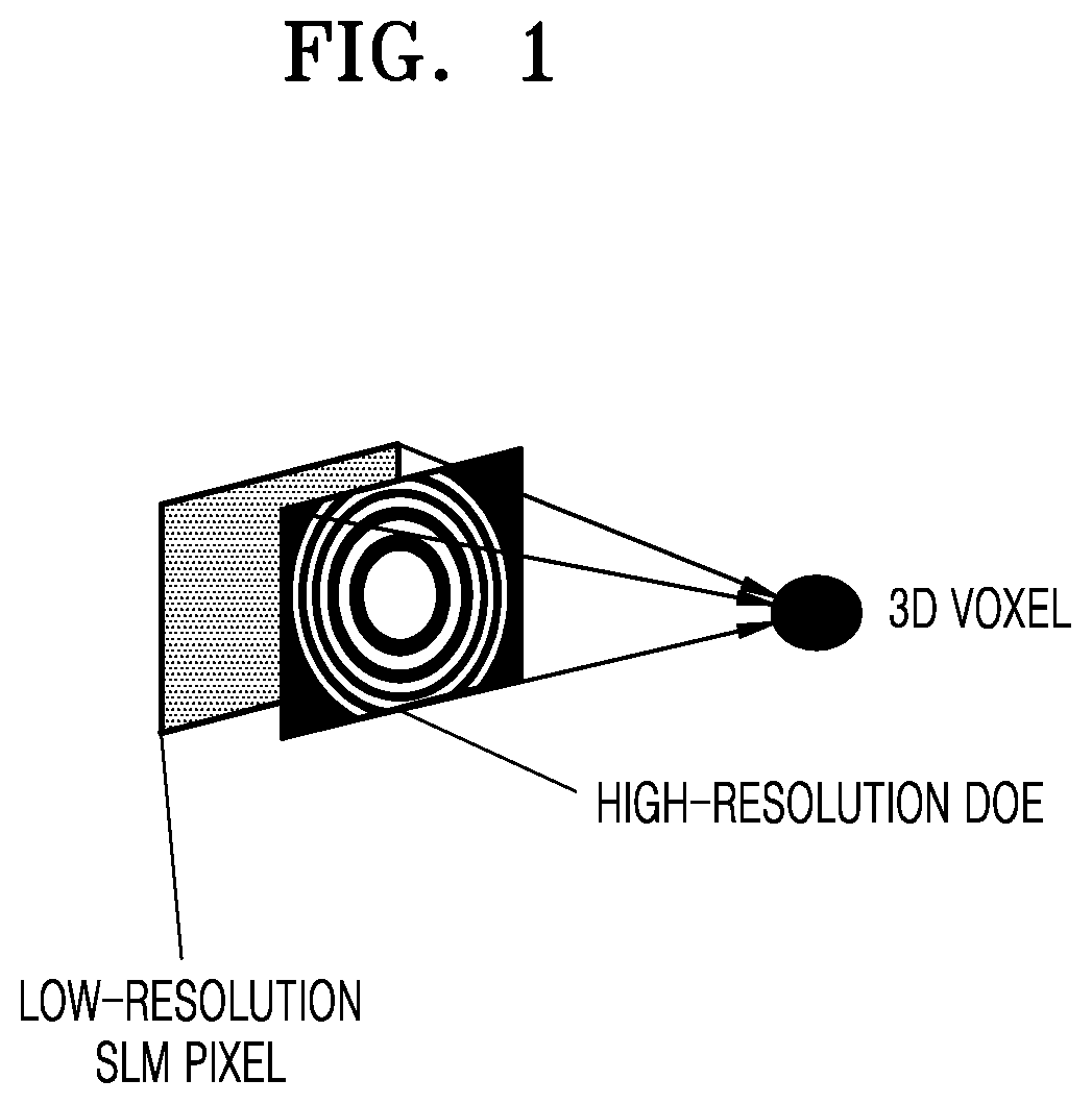
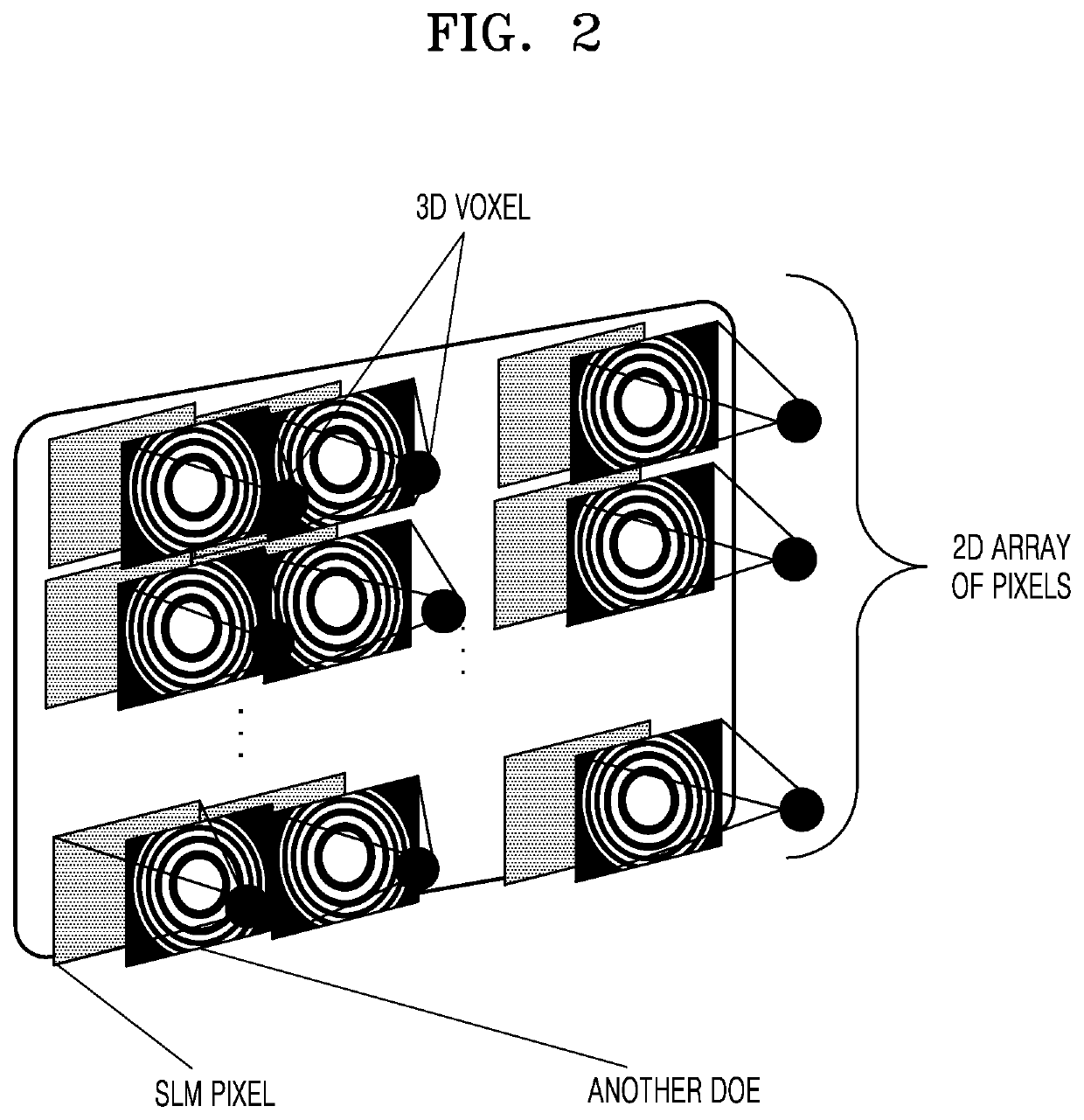
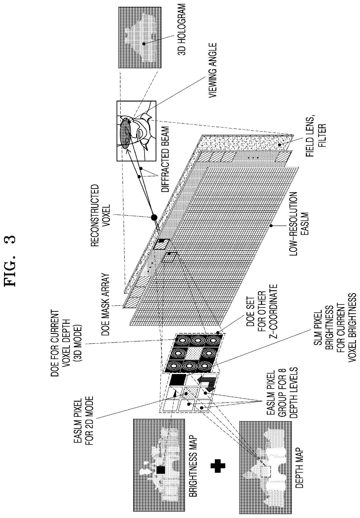
[0013]An example embodiment provides a compact holographic display.

[0014]An example embodiment provides a method, performed by a holographic display, of forming a holographic image.

Solution To Problem

[0015]According to an embodiment, a holographic display may include

[0016]an electrically addressable spatial light modulator (EASLM);

[0017]a diffractive optical element (DOE) mask array arranged on the EASLM; and

[0018]a controller configured to operate the holographic display to form a hologram image,

[0019]wherein the controller is further configured to address the EASLM to backlight the DOE mask array required to form a set of hologram image voxels by turning on a corresponding EASLM pixel.

[0020]The EASLM may be a non-coherent EASLM.

[0021]The holographic display may further include an optically addressable spatial light modulator (OASLM) and a backlight unit, and the EASLM, the DOE mask array, and the OASLM may be integrated into a single unit.

[0022]The OASLM may inclu...


PUM

PropertyMeasurementUnit
sizeaaaaaaaaaa
sizeaaaaaaaaaa
pixel sizeaaaaaaaaaa

Abstract

A holographic display and a method, performed by the holographic display, of forming a holographic image are disclosed. The holographic display includes an electrically addressable spatial light modulator (EASLM); a diffractive optical element (DOE) mask array arranged on the EASLM; and a controller configured to operate the holographic display to form a hologram image, wherein the controller is further configured to address the EASLM to backlight the DOE mask array required to form a set of hologram image voxels by turning on a corresponding EASLM pixel.

Description

TECHNICAL FIELD[0001]The disclosure relates to the forming of holographic images, and more particularly, to a holographic display and a method, performed by a holographic display, of forming a holographic image.BACKGROUND ART[0002]The forming of three-dimensional (3D) hologram images (holograms) has great potential in many fields of applications, such as telecommunications, medicine, entertainment, military equipment, or the like. However, there are many problems with the large-area implementation using the technique.[0003]Holographic displays that are currently available have large sizes due to optical systems of high quality required for the reproduction of digital holograms displayed on an electrically addressable spatial light modulator (EASLM). This increases the size of holographic images and makes the holographic images almost impossible to be integrated into a wearable smart device (a watch, a phone, a tablet, or the like).[0004]Current holographic displays do not provide su...

Claims


Application Information

Patent Timeline
Patent Type & Authority Applications(United States)
IPC IPC(8): G03H1/22G02F1/1333
CPCG02F2203/12G03H2225/60G02F1/133362G02F2203/50G03H2225/25G03H1/2294G03H2225/22G03H1/2205G03H2223/23G03H2225/32G02F1/133504G02F1/133526G02F1/1336G03H2001/0224G03H2001/0212G03H2001/0216G03H2001/221G03H2001/2223G03H2001/261G03H2001/264G03H1/30G03H2001/306G03H2210/452G03H2222/34G03H2223/12G03H2223/13G03H2223/14G03H2223/17G03H2225/12G03H2225/23G03H2225/55H01L25/167G03H2001/0825G03H1/2202G03H1/0808G03H1/2286H01L27/14625G02F1/133601G02F1/133562H10K59/00G03H1/268G03H2210/30G03H1/02
Inventor POPOV, MIKHAIL VYACHESLAVOVICHSHTYKOV, STANISLAV ALEKSANDROVICHSHESTAK, SERGEY ALEKSANDROVICHHWANG, SEONDEOK
Owner SAMSUNG ELECTRONICS CO LTD
Why Eureka
Try Eureka