Supercharge Your Innovation With Domain-Expert AI Agents!

Pixel array substrate including flux structure layer for improving LED contact and method of manufacturing thereof

a technology of flux structure layer and pixel array substrate, which is applied in the direction of semiconductor devices, semiconductor/solid-state device details, instruments, etc., can solve the problems of many technical bottlenecks to be overcome, and the micro light-emitting diodes on the pixel array substrate cannot function normally, so as to increase the probability

Active Publication Date: 2021-01-14
AU OPTRONICS CORP
View PDF0 Cites 2 Cited by
  • Summary
  • Abstract
  • Description
  • Claims
  • Application Information

AI Technical Summary

Benefits of technology

Enhances the probability of correct electrical connections between micro light-emitting diodes and contact pads, reduces light reflections, and improves display quality by maintaining light extraction efficiency and preventing flux material overlap on contact pads.

Problems solved by technology

However, there are still many technical bottlenecks to be overcome in the development of micro-LED displays, among which the most important is “Mass Transfer” technology.
In the prior art, micro light-emitting diodes often shift during transposition, resulting in that the micro light-emitting diodes on the pixel array substrate cannot function normally.

Method used


Image

  • Pixel array substrate including flux structure layer for improving LED contact and method of manufacturing thereof
  • Pixel array substrate including flux structure layer for improving LED contact and method of manufacturing thereof
  • Pixel array substrate including flux structure layer for improving LED contact and method of manufacturing thereof

Examples


Embodiment Construction

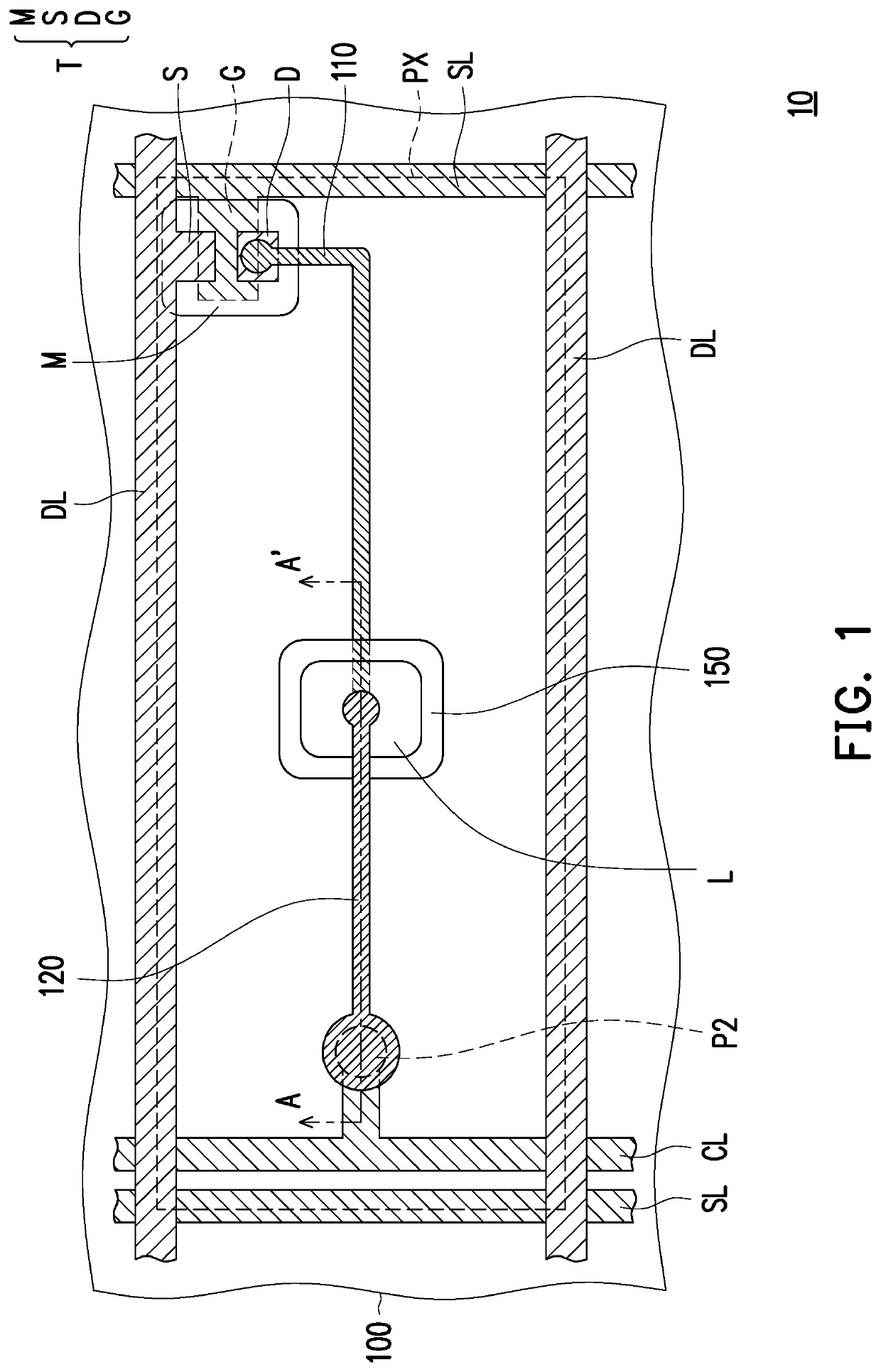
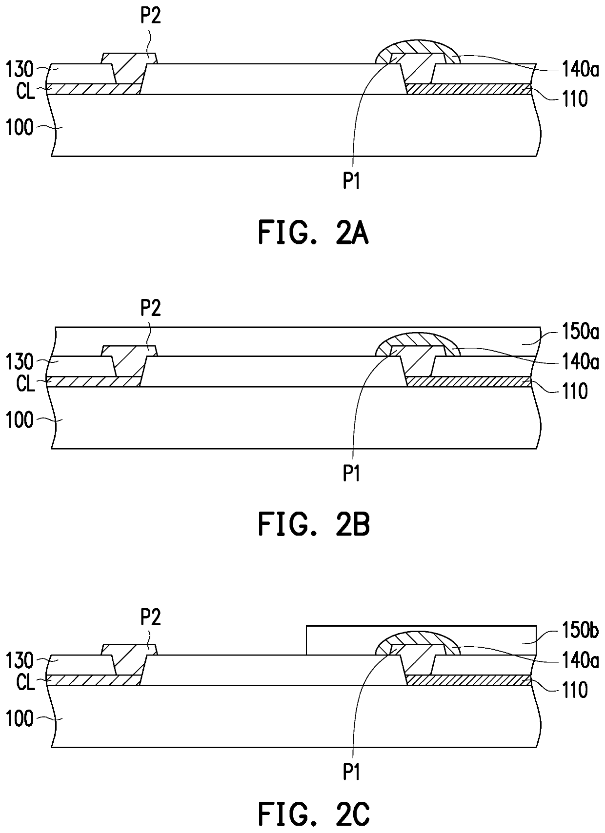
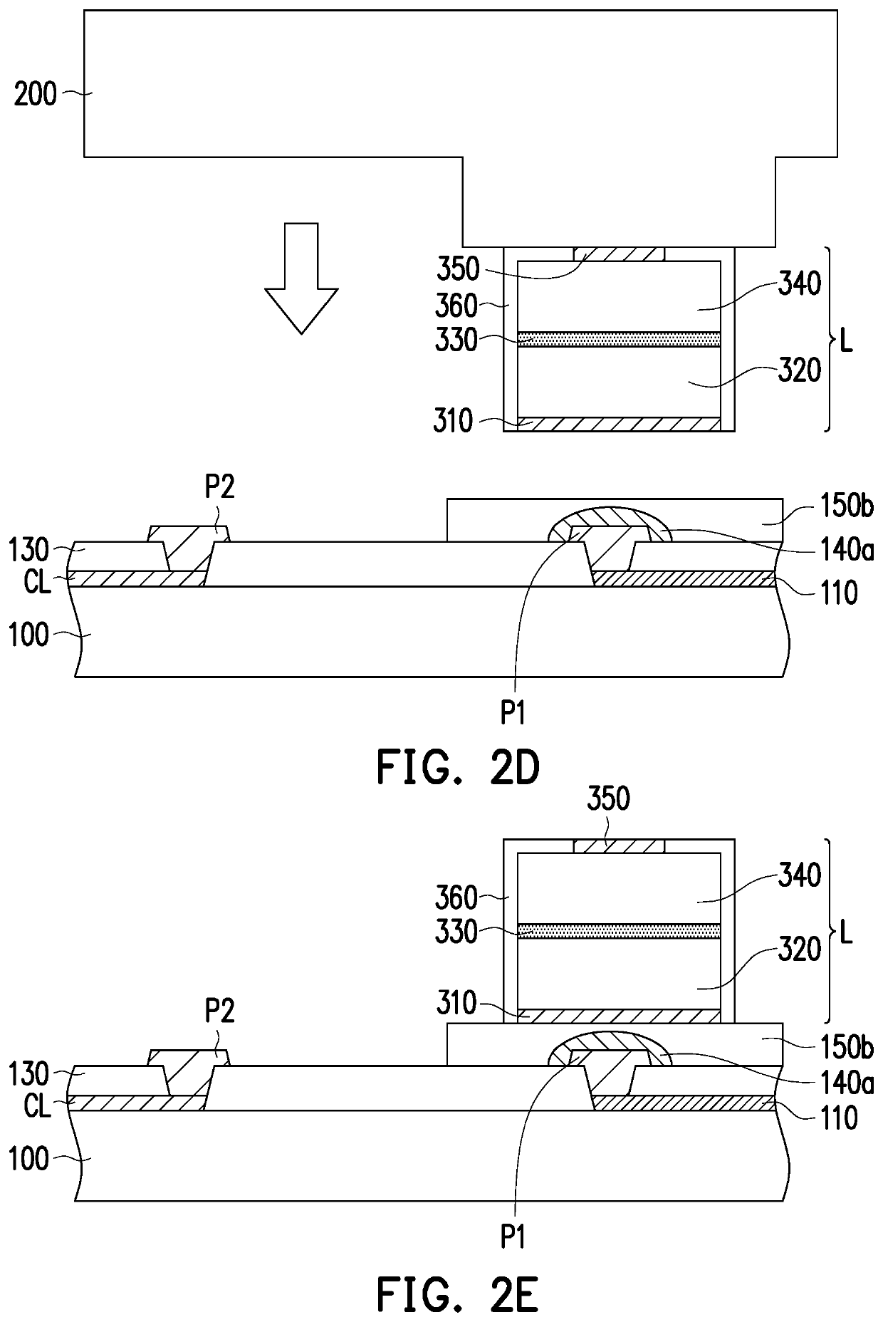
[0017]FIG. 1 is a schematic top view of a pixel array substrate 10 according to an embodiment of the invention. FIGS. 2A-2G are schematic cross-sectional views showing a manufacturing process of a pixel array substrate according to an embodiment of the invention. For example, FIGS. 2A-2G are schematic views of the manufacturing process in view of the cross-section of line AA′ of FIG. 1. In FIG. 1, some components are omitted.

[0018]Referring to FIG. 1, the pixel array substrate 10 includes a substrate 100. The substrate 100 has a sub-pixel region PX, and a pixel structure is disposed within the sub-pixel region PX. Although FIG. 1 shows only one sub-pixel region PX, the invention is not limited thereto. The substrate 100 actually includes a plurality of sub-pixel regions PX. The range of the single sub-pixel region PX is defined by two adjacent transmission lines having the same function and two adjacent conductive wires having the same function, and the transmission lines and the co...


PUM

PropertyMeasurementUnit
temperatureaaaaaaaaaa
heightaaaaaaaaaa
distanceaaaaaaaaaa

Abstract

A pixel array substrate has a plurality of sub-pixel regions, wherein a pixel structure of an individual sub-pixel region includes a first signal line, a second signal line, a first contact pad, a second contact pad, a light-emitting diode, a first conductive structure, and a flux structure layer. The first contact pad and the second contact pad are respectively electrically connected with the first signal line and the second signal line. The light-emitting diode is disposed on the first contact pad. A portion of the first conductive structure is disposed between the first contact pad and a first electrode of the light-emitting diode. The flux structure layer partially surrounds the first conductive structure and the light-emitting diode. A top portion of the flux structure layer is higher than a top surface of the first electrode and is lower than a bottom surface of a light-emitting layer of the light-emitting diode.

Description

CROSS-REFERENCE TO RELATED APPLICATION[0001]This application is a divisional application of and claims the priority benefit of U.S. application Ser. No. 16 / 183,719, filed on Nov. 7, 2018, now allowed. The prior U.S. application Ser. No. 16 / 183,719 claims the priority benefit of Taiwan application serial no. 106143799, filed on Dec. 13, 2017. The entirety of each of the above-mentioned patent applications is hereby incorporated by reference herein and made a part of specification.BACKGROUNDTechnical Field[0002]The invention relates to a pixel array substrate, and more particularly, to a pixel array substrate having a flux structure layer.Description of Related Art[0003]Currently, in common liquid crystal displays, the light-emitting diode (LED) plays the role of providing a backlight source, and can use a liquid crystal as a light switch. With the progress of science and technology, display technology has gradually changed from backlighting to self-luminescence. Micro-LED displays fu...

Claims


Application Information

Patent Timeline
Patent Type & Authority Applications(United States)
IPC IPC(8): H01L33/62H01L25/075
CPCH01L33/62H01L25/0753H01L2224/18H01L2224/81H01L2933/0066G02F1/1362H01L23/5386H01L24/83H01L2224/832H01L2224/83024
Inventor YU, FANG-CHENGTSAI, CHENG-YEH
Owner AU OPTRONICS CORP
Features
  • R&D
  • Intellectual Property
  • Life Sciences
  • Materials
  • Tech Scout
  • Unparalleled Data Quality
  • Higher Quality Content
  • 60% Fewer Hallucinations
Learn More