
High frequency amplifier circuit and communication device

Active Publication Date: 2021-01-14
MURATA MFG CO LTD
View PDF0 Cites 1 Cited by
  • Summary
  • Abstract
  • Description
  • Claims
  • Application Information

AI Technical Summary

Benefits of technology

The present patent offers a circuit and device that can amplify signals in a wide range of frequencies with good quality. This improves the overall performance of the communication device.

Problems solved by technology

For this reason, as in the multiband communication device described in Japanese Unexamined Patent Application Publication No. 2004-320446, when attempting to cope with wide communication bands, such as n77 by one power amplifier or one low-noise amplifier for each communication band, it is difficult to ensure good amplification characteristics in the entire communication band, and the amplification characteristics deteriorate.

Method used


Image

  • High frequency amplifier circuit and communication device
  • High frequency amplifier circuit and communication device
  • High frequency amplifier circuit and communication device

Examples


embodiments

1.1 Configuration of Communication Device

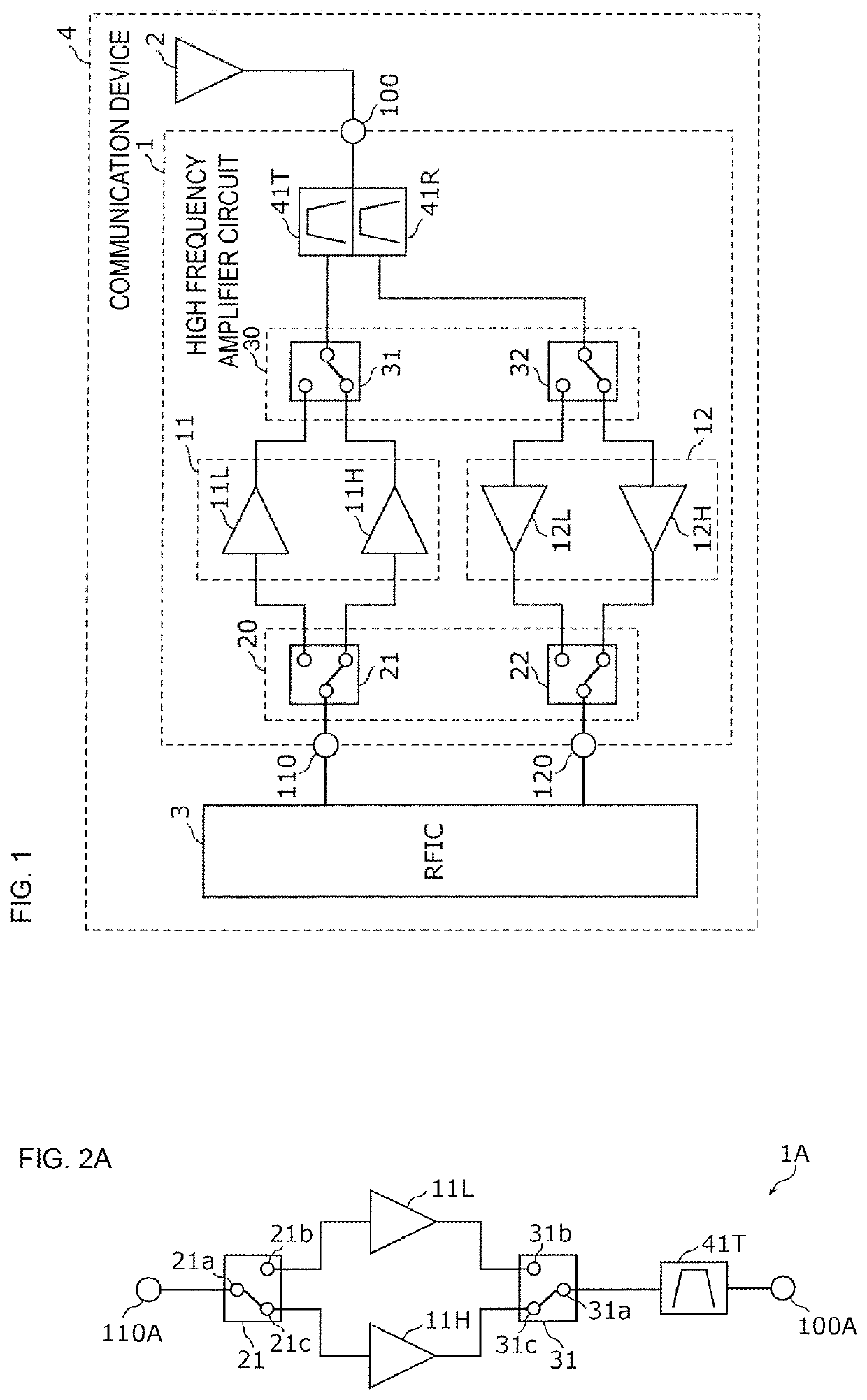
[0017]FIG. 1 is a circuit configuration diagram of a communication device 4 according to an embodiment. As illustrated in the figure, the communication device 4 includes an antenna element 2, a high frequency amplifier circuit 1, and an RF signal processing circuit (RFIC) 3.

[0018]The RFIC 3 is an RF signal processing circuit that processes a high frequency signal transmitted and received by the antenna element 2. Specifically, the RFIC 3 performs signal processing on a high frequency reception signal input via a reception path of the high frequency amplifier circuit 1 by down-conversion or the like, and outputs a reception signal generated by the signal processing to a baseband signal processing circuit (not illustrated) or the like. In addition, the RFIC 3 performs signal processing on a transmission signal input from the baseband signal processing circuit or the like by up-conversion or the like, and outputs a high frequency transmission si...


PUM


Abstract

A high frequency amplifier circuit includes an input terminal and an output terminal, transmission power amplifiers (11L, 11H) that amplify a high frequency signal in first and second frequency bands, each of which is a part of a communication band, at equal to or higher than a prescribed amplification factor, respectively, switches (21, 31) that exclusively switch connection between the input terminal, the transmission power amplifier (11L), and the output terminal, and connection between the input terminal, the transmission power amplifier (11H), and the output terminal, and a transmission filter that is connected between the output terminal and the switch (31) and has a communication band as a pass band, the first frequency band including a frequency band other than the second frequency band, the second frequency band including a frequency band other than the first frequency band.

Description

[0001]This is a continuation of International Application No. PCT / JP2019 / 023392 filed on Jun. 13, 2019 which claims priority from Japanese Patent Application No. 2018-116342 filed on Jun. 19, 2018. The contents of these applications are incorporated herein by reference in their entireties.BACKGROUND[0002]The present disclosure relates to a high frequency amplifier circuit and a communication device.[0003]In recent years, it has been desired to amplify high frequency signals of a plurality of communication bands with high gain and low noise in a high frequency amplifier circuit for a mobile communication device corresponding to multi-band / multi-mode.[0004]Japanese Unexamined Patent Application Publication No. 2004-320446 (FIG. 2) discloses a multiband communication device including an antenna duplexer, a first power amplifier and a second power amplifier, and a first low-noise amplifier and a second low-noise amplifier. In the above-described multiband communication device, in each o...

Claims


Application Information

Patent Timeline
IPC IPC(8): H03F1/42H04B1/40H03F3/24
CPCH03F1/42H04B1/40H03F3/245H03F2200/36H03F2200/165H03F2200/171H03F2200/294H03F2200/451H03F3/195H03F3/72H03F2203/7209H03F2200/111H04B2001/0408H04B1/006
Inventor ONO, ATSUSHI
Owner MURATA MFG CO LTD
Learn More