Memory device

Active Publication Date: 2021-01-28
FUJIAN JINHUA INTEGRATED CIRCUIT CO LTD
View PDF0 Cites 2 Cited by
  • Summary
  • Abstract
  • Description
  • Claims
  • Application Information

AI Technical Summary

Benefits of technology

[0011]Furthermore, the lower portions of the node contact windows that extend in the substrate may, for example, include respective first grooves formed in trench isolation structures and respective second grooves formed in the active ar

Problems solved by technology

In the state of the art, the existing memory devices are still faced with a number of challenges including difficult and tedious fabrication.
These strict requirements

Method used


Image

  • Memory device
  • Memory device
  • Memory device

Examples


Embodiment Construction

[0039]Specific embodiments of the memory device proposed in this invention will be described in greater detail below with reference to the accompanying drawings. Features and advantages of the invention will be more apparent from the following detailed description. Note that the accompanying drawings are provided in a very simplified form not necessarily presented to scale, with their only intention to facilitate convenience and clarity in explaining the embodiments.

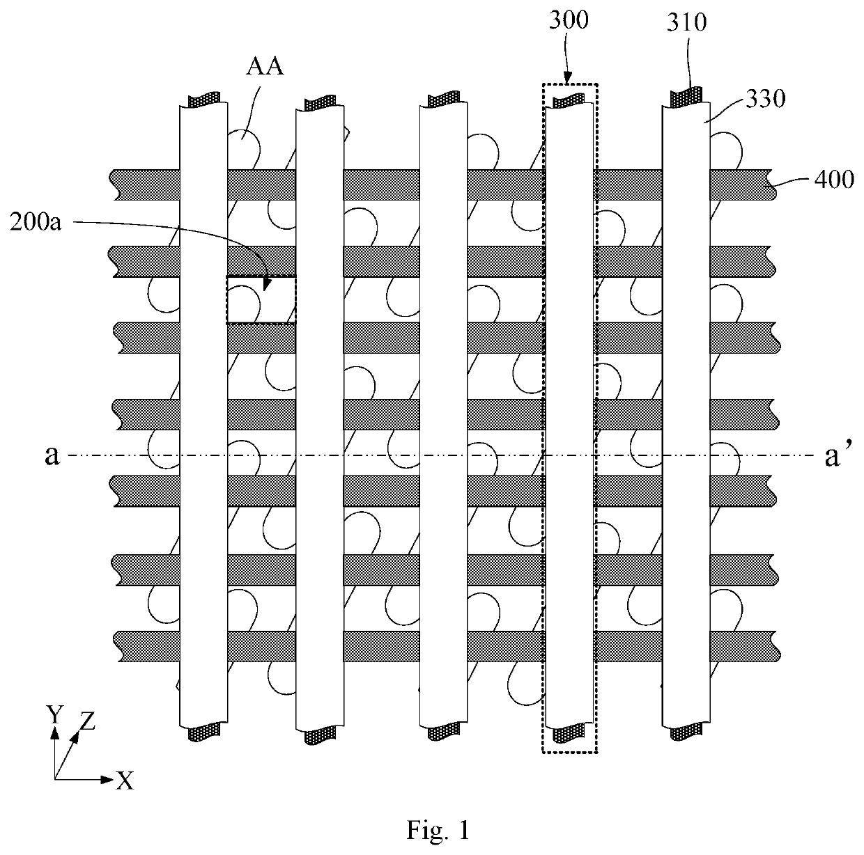
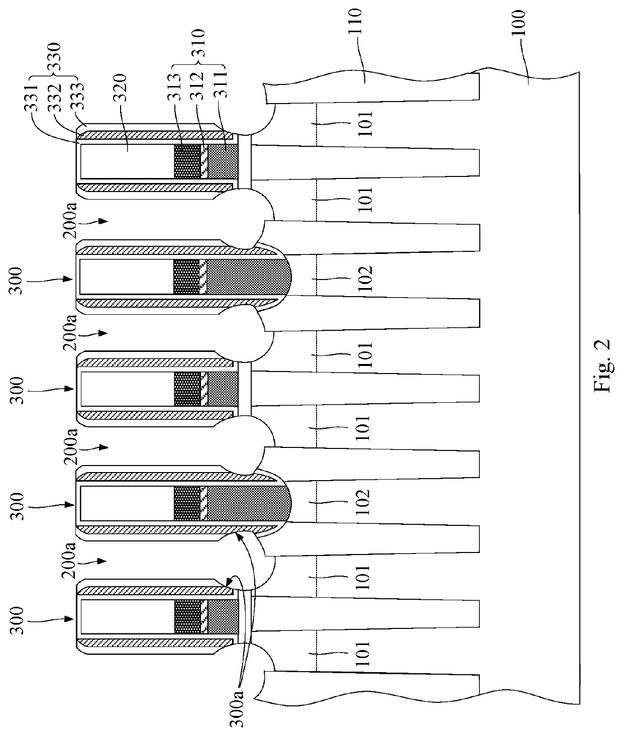
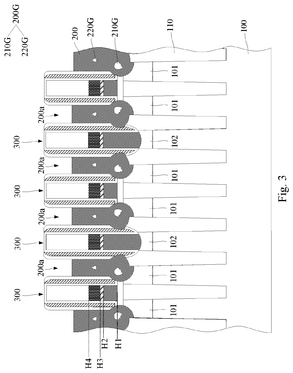
[0040]FIG. 1 is a top view of a memory device according to an embodiment of the present invention. FIG. 2 is a schematic cross-sectional view of a memory device according to an embodiment of the invention taken along line aa′, in which node contacts are not shown. FIG. 3 is a schematic cross-sectional view of a memory device according to an embodiment of the invention taken along line aa′. It is noted that, for the sake of a clearer understanding of the invention, some components are not shown in the top view of FIG. 1, ...


PUM


Abstract

A memory device is disclosed, in which node contacts extend into a substrate, where they are come into electrical connection with active areas. This allows greater contact areas between the node contacts and the active areas and electrical connection of the node contacts with high ion concentration portions of the active areas. As a result, even when voids are formed in the node contacts, the node contacts can still possess desired connection performance. For node contacts allowed to contain voids, this enables them to be fabricated faster with lower difficulty, thus increasing manufacturing throughput of the memory device.

Description

TECHNICAL FIELD[0001]The present invention relates to the field of semiconductor technology and, in particular, to a memory device.BACKGROUND[0002]A memory device, such as a dynamic random access memory (DRAM) device, typically includes storage capacitors and storage transistors electrically connected to the storage capacitors. The storage capacitors are adapted to hold charges representative of information stored thereon, and the storage transistors may be electrically coupled to the storage capacitors via node contacts.[0003]In the state of the art, the existing memory devices are still faced with a number of challenges including difficult and tedious fabrication. For example, in order to form a node contact ensured to be electrically connected with good quality to a storage transistor, the processes used must meet very stringent requirements, such as a deposition process with good filling performance. These strict requirements inevitably slow down the node contact's fabrication, ...

Claims


Application Information

Patent Timeline
IPC IPC(8): G11C11/4097H01L27/108
CPCG11C11/4097H01L27/108H10B12/34H10B12/30H10B12/00
Inventor WANG, JIANFANGGUO, PENGLI, BAOYUWANG, YUANBAO
Owner FUJIAN JINHUA INTEGRATED CIRCUIT CO LTD
Why Eureka
Try Eureka