Semiconductor structure and method for forming the same, and a transistor

a technology of semiconductors and transistors, applied in the field of semiconductor manufacturing, can solve the problems of increasing the critical dimension of mos transistors, and achieve the effects of improving the forming quality of metal gate structures, reducing difficulty, and increasing the top opening of gate openings

Active Publication Date:
View PDF0 Cites 4 Cited by
  • Summary
  • Abstract
  • Description
  • Claims
  • Application Information

AI Technical Summary

Benefits of technology

[0010]Embodiments and implementations of the present disclosure provide a method for forming a semiconductor structure, including: removing the portion of the height of the dummy gate layer to form the remaining dummy gate layer, where the remaining dummy gate layer and the spacer enclose the trench; thinning the spacer exposed from the remaining dummy gate layer along the direction perpendicular to the side wall of the trench; and after the thinning, removing the remaining dummy gate layer to form the gate opening within the interlayer dielectric layer. Therefore, through the thinning, the T-shaped gate opening of the remaining spacer is formed on the side wall, so that a dimension of a top opening of the gate opening is increased, thereby reducing difficulty in forming the metal gate structure within the gate opening, and correspondingly helping to improve forming quality of the metal gate structure within the gate opening, and further improving performance of the formed transistor.
[0011]In some implementations, after forming a metal gate structure in the gate opening, the method further includes: removing a high-k gate dielectric layer and a top spacer that are located over the bottom spacer, to form a trench enclosed by the interlayer dielectric layer, the bottom spacer, and a remainder of the metal gate structure, and forming an etch blocking layer in the trench, where a source / drain doped region is usually formed within a base on both sides of the metal gate structure. In addition, the method for forming the semiconductor structure may further include: forming a contact plug within the interlayer dielectric layer on both sides of the metal gate structure, where the contact plug is electrically connected to the source / drain doped region. In embodiments and implementations of the present disclosure, the etch blocking layer is formed, helping to enlarge a process window for forming the contact plug, correspondingly reducing a probability of bridging between the contact plug and the metal gate structure, and improving an effect of electrical isolation between the contact plug and the metal gate structure, thereby further improving performance of the formed transistor.
[0012]In some implementations, after forming a trench and before forming an etch blocking layer in the trench, the method further includes: removing a portion of a height of a remainder of the metal gate structure, where after the etch blocking layer is formed in the trench, the etch stop layer correspondingly further covers a top of the remainder of the metal gate structure. Therefore, in a manufacturing procedure of forming the contact plug, the etch blocking layer on the top of the remainder of the metal gate structure can protect the top of the remainder of the metal gate structure, further enlarging the process window for forming the contact plug. For example, a self-aligned contact (SAC) etching process may be used.

Problems solved by technology

With the continuous development of integrated circuit manufacturing technologies, a critical dimension of the MOS transistor becomes increasingly small, and various secondary effects caused by physical limits of devices appear successively, impeding scaling down of a critical dimension of the device.
One of the most challenging problems is to alleviate large current leakage of a semiconductor device.

Method used


Image

  • Semiconductor structure and method for forming the same, and a transistor
  • Semiconductor structure and method for forming the same, and a transistor
  • Semiconductor structure and method for forming the same, and a transistor

Examples


Embodiment Construction

[0016]A performance of current transistors can be improved. Reasons why the performance of a transistor is still to be improved are now analyzed in combination with a semiconductor structure.

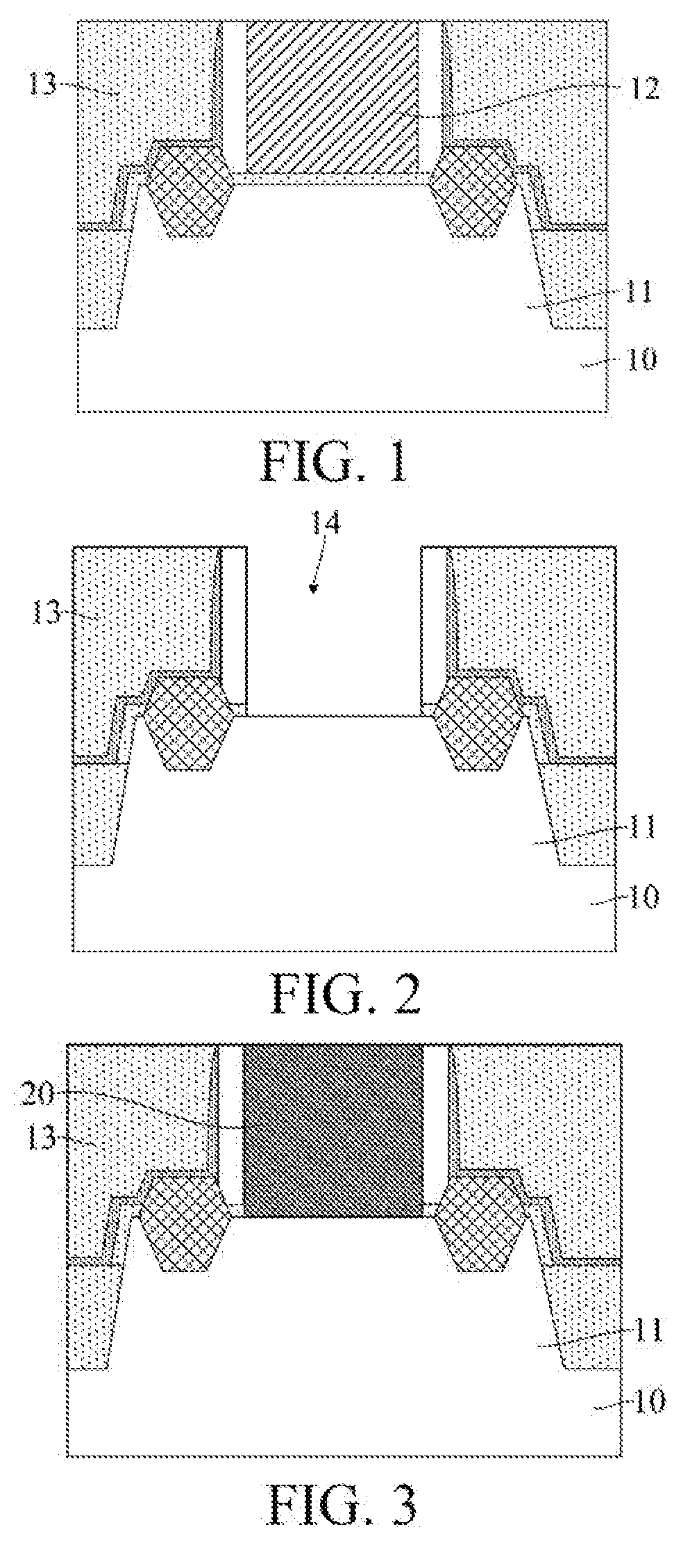
[0017]FIG. 1 to FIG. 3 illustrate respective schematic structural diagrams of steps in a method for forming a semiconductor structure are shown.

[0018]Referring to FIG. 1, a substrate 10 and a fin 11 protruding from the substrate 10 are provided, where a dummy gate layer 12 across the pin 11 is formed on the substrate 10, an interlayer dielectric layer 13 is formed on the substrate 10 exposed from the dummy gate layer 12, and the interlayer dielectric layer 13 exposes a top of the dummy gate layer 12.

[0019]Referring to FIG. 2, the dummy gate layer 12 is removed, to form a gate opening 14 within the interlayer dielectric layer 13.

[0020]Referring to FIG. 3, a metal gate structure 20 is formed within the gate opening 14.

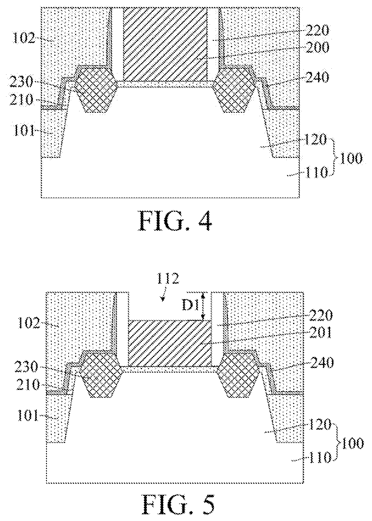
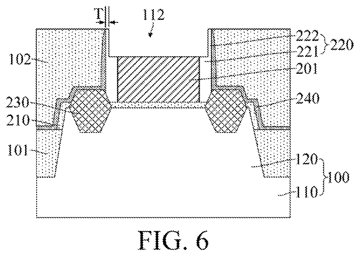
[0021]With continuous reduction of a critical dimension of an integrated circuit...


PUM

PropertyMeasurementUnit
heightaaaaaaaaaa
thicknessaaaaaaaaaa
distanceaaaaaaaaaa

Abstract

A semiconductor structure and a method for forming the same, and a transistor are provided. In one form, a method includes: providing a base, where a dummy gate layer is formed on the base, a spacer is formed on a side wall of the dummy gate layer, an interlayer dielectric layer is formed on the base exposed from the dummy gate layer and the spacer, and the interlayer dielectric layer exposes a top of the dummy gate layer and a top of the spacer; removing a portion of a height of the dummy gate layer to form a remaining dummy gate layer, where the remaining dummy gate layer and the spacer enclose a trench; thinning a spacer exposed from the remaining dummy gate layer along a direction perpendicular to a side wall of the trench; after the thinning, removing the remaining dummy gate layer to form a gate opening within the interlayer dielectric layer; and forming a metal gate structure in the gate opening. Through the thinning, a gate opening whose side wall is provided with a remaining spacer is T-shaped. That is, a dimension of a top opening of the gate opening is increased, so that difficulty in forming the metal gate structure within the gate opening is reduced. That is, forming quality of the metal gate structure within the gate opening is helped to be improved, thereby improving performance of the transistor.

Description

RELATED APPLICATIONS[0001]The present application claims priority to Chinese Patent Appln. No. 201910697155.8, filed Jul. 30, 2019, the entire disclosure of which is hereby incorporated by reference.BACKGROUNDTechnical Field[0002]Embodiments and implementations of the present disclosure relate to the field of semiconductor manufacturing, and in particular, to a semiconductor structure and a method for forming the same, and a transistor.Related Art[0003]A main semiconductor device of an integrated circuit, especially a super-large-scale integrated circuit, is a metal-oxide-semiconductor field effect transistor (MOS transistor). With the continuous development of integrated circuit manufacturing technologies, a critical dimension of the MOS transistor becomes increasingly small, and various secondary effects caused by physical limits of devices appear successively, impeding scaling down of a critical dimension of the device. One of the most challenging problems is to alleviate large c...

Claims


Application Information

Patent Timeline
Patent Type & Authority Applications(United States)
IPC IPC(8): H01L21/768H01L21/311H01L29/66H01L21/762
CPCH01L21/76831H01L21/76802H01L21/76224H01L29/66545H01L21/76837H01L21/31116H01L29/6653H01L29/7838H01L29/42376H01L29/6656H01L29/66795H01L29/7848H01L29/4966H01L21/28114H01L21/28088
Inventor ZHOU, FEI
Why Eureka
Try Eureka