Semiconductor device and high-frequency module

a technology of semiconductor devices and high-frequency modules, which is applied in the direction of semiconductor devices, semiconductor/solid-state device details, electrical apparatus, etc., can solve the problems of hbt being damaged accordingly and stress can be added to hbt, so as to achieve the effect of low thermal stress and highly reliable semiconductor devices

Active Publication Date: 2021-02-04
MURATA MFG CO LTD
View PDF0 Cites 5 Cited by
  • Summary
  • Abstract
  • Description
  • Claims
  • Application Information

AI Technical Summary

Benefits of technology

[0004]The semiconductor device disclosed in Japanese Unexamined Patent Application Publication No. 2003-77930 described above is face-down mounted over a mounting board for example. After the mounting, the semiconductor device undergoes resin sealing. In the mounting process of the semiconductor device, heating treatment, such as reflow treatment, is performed. In the heating treatment, thermal stress due to a difference in coefficient of linear expansion between the semiconductor portion and metal wiring of the semiconductor device occurs near an interface where the semiconductor portion and the metal wiring are in

Problems solved by technology

The thermal stress can be added to the HB

Method used


Image

  • Semiconductor device and high-frequency module
  • Semiconductor device and high-frequency module
  • Semiconductor device and high-frequency module

Examples


first embodiment

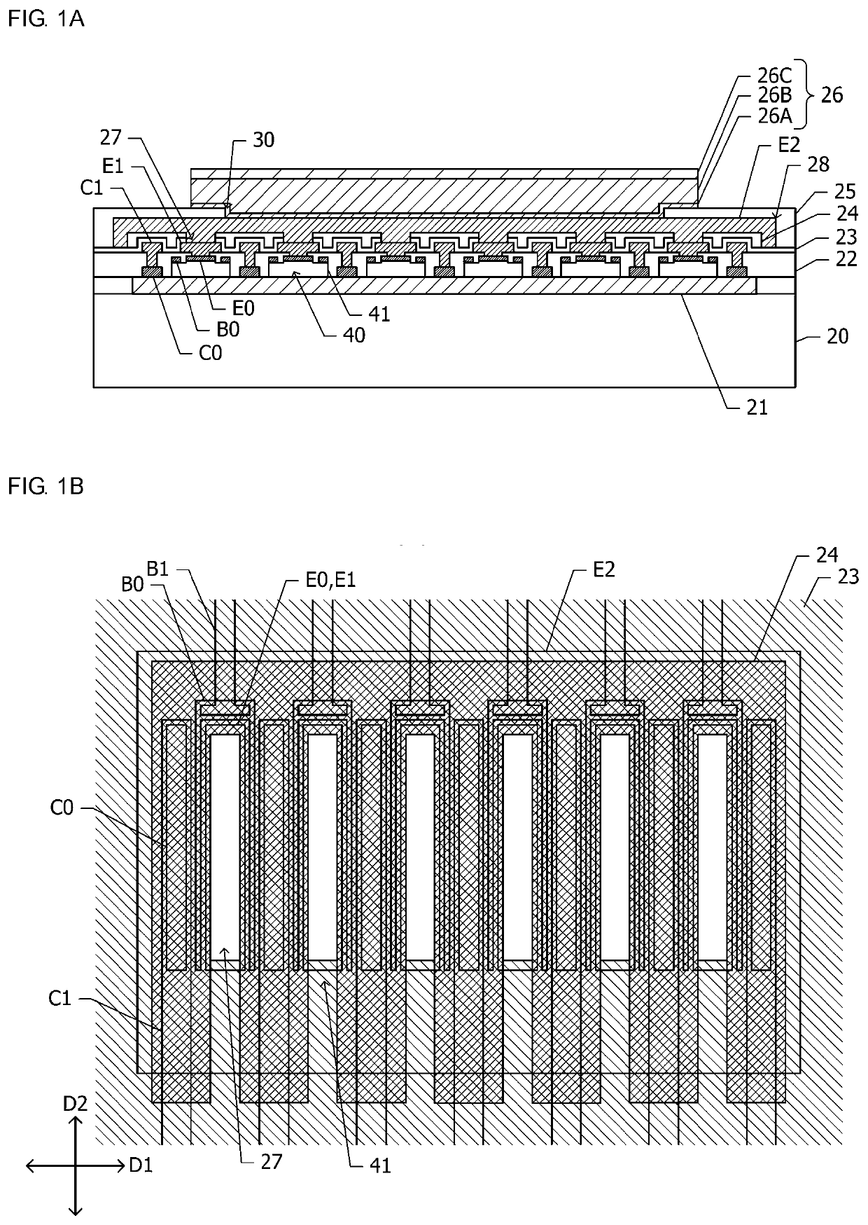
[0027]With reference to FIG. 1A and FIG. 1B, a semiconductor device according to a first embodiment is described.

[0028]FIG. 1A is a cross-sectional view of the semiconductor device according to the first embodiment. A sub-collector layer 21 having n-type conductivity is arranged in an outer surface portion of a substrate 20. A plurality of unit transistors 40, the number of which is six for example, are formed on the sub-collector layer 21. The plurality of unit transistors 40 are mutually coupled in parallel. Each of the unit transistors 40 is constituted by a mesa-like multilayer body 41, which is arranged on the sub-collector layer 21. The mesa-like multilayer body 41 includes a collector layer, a base layer, and an emitter layer, which are laminated in order from the side of the substrate. A pn junction interface between the base layer and the collector layer lies throughout the region of the mesa-like multilayer body 41 in a plan view while a pn junction interface between the e...

second embodiment

[0053]With reference to FIGS. 2 to 6, a semiconductor device 50 and a high-frequency module according to a second embodiment is described below. Hereinafter, the description of a configuration common to the semiconductor device according to the first embodiment is omitted.

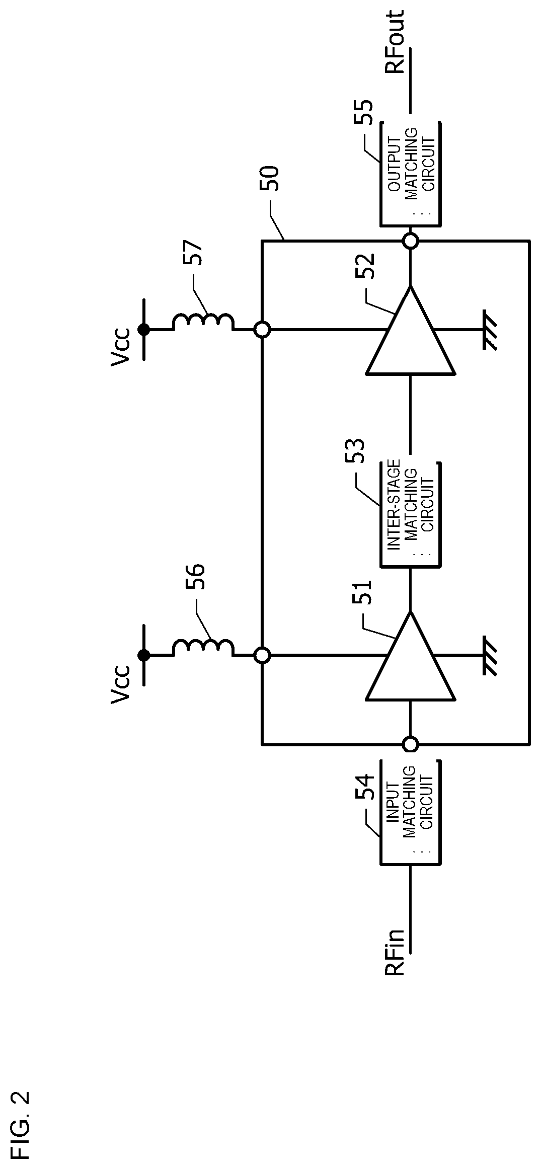
[0054]FIG. 2 is a block diagram of the high-frequency module in which the semiconductor device 50 according to the second embodiment is used. The high-frequency module includes a driver-stage amplification circuit 51, an output-stage amplification circuit 52, an inter-stage matching circuit 53, an input matching circuit 54, an output matching circuit 55, and inductors 56 and 57. The driver-stage amplification circuit 51, the output-stage amplification circuit 52, the inter-stage matching circuit 53, and the like are integrated in the semiconductor device 50. A bias circuit is not illustrated in FIG. 2. Supply voltage Vcc is supplied to the driver-stage amplification circuit 51 and the output-stage amplification cir...

third embodiment

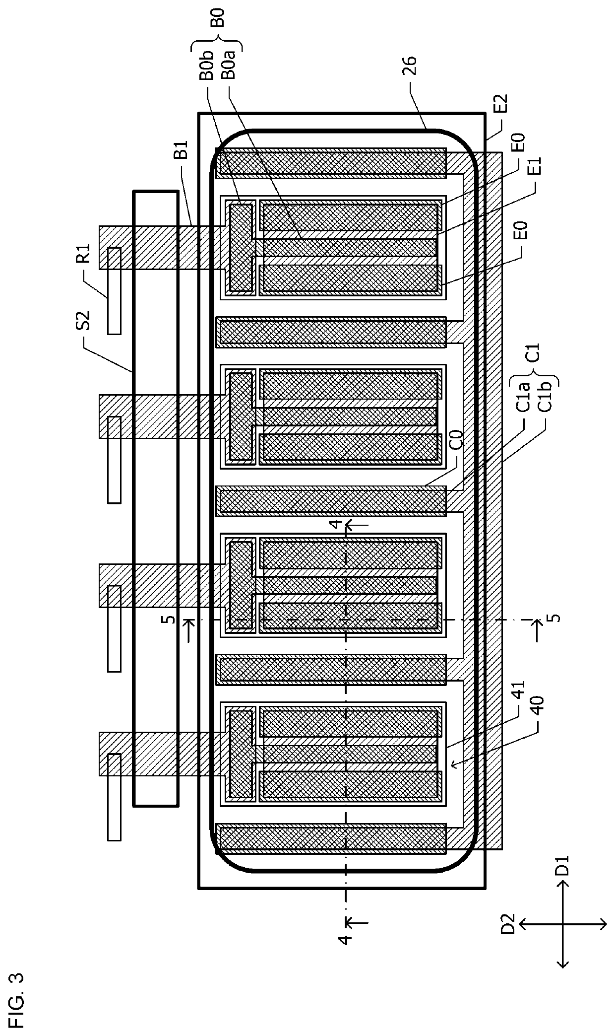
[0089]With reference to FIG. 9, a semiconductor device according to a third embodiment is described below. Hereinafter, the description of a configuration common to the semiconductor device according to the second embodiment (FIGS. 3 to 6) is omitted.

[0090]FIG. 9 illustrates a positional relation between an inorganic insulation film 23 and an organic insulation film 24, and other components according to the third embodiment in a plan view. In FIG. 9, the inorganic insulation film 23 is given a hatch pattern drawn downward to the right, which is relatively low in density, while the organic insulation film 24 is given a hatch pattern drawn upward to the right, which is relatively high in density.

[0091]In the third embodiment, openings 29 that include openings 27 in the inorganic insulation film 23 in a plan view are provided in the organic insulation film 24. In FIG. 9, the regions with no hatch patterns correspond to the openings 27 and the regions with no hatch patterns or only with...


PUM


Abstract

At least one unit transistor is arranged over a substrate. A first wiring as a path of current that flows to each unit transistor is arranged over the at least one unit transistor. An inorganic insulation film is arranged over the first wiring. At least one first opening overlapping a partial region of the first wiring in a plan view is provided in the inorganic insulation film. An organic insulation film is arranged over the inorganic insulation film. A second wiring coupled to the first wiring through the first opening is arranged over the organic insulation film and the inorganic insulation film. In a plan view, a region in which the organic insulation film is not arranged is provided outside a region in which the first wiring is arranged. The second wiring is in contact with the inorganic insulation film outside the region in which the first wiring is arranged.

Description

CROSS-REFERENCE TO RELATED APPLICATIONS[0001]This application claims benefit of priority to Japanese Patent Application No. 2019-141341, filed Jul. 31, 2019, and to Japanese Patent Application No. 2020-074812, filed Apr. 20, 2020, the entire contents of each are incorporated herein by reference.BACKGROUNDTechnical Field[0002]The present disclosure relates to semiconductor devices and high-frequency modules.Background Art[0003]Japanese Unexamined Patent Application Publication No. 2003-77930, described below, discloses a semiconductor device including a heterojunction bipolar transistor (HBT). The semiconductor device includes the HBT, which is formed on a semiconductor substrate, and a bump for external coupling. An emitter electrode is coupled to the emitter of the HBT and wiring of the first layer is arranged over the emitter electrode. The bump is arranged over the wiring. An insulation film is arranged between the emitter electrode and the wiring of the first layer while an insu...

Claims


Application Information

Patent Timeline
IPC IPC(8): H01L23/00H01L29/737H01L27/082H01L23/498H01L23/66
CPCH01L23/562H01L29/7371H01L27/0823H01L24/13H01L24/16H01L23/49838H01L2924/351H01L2224/13026H01L2224/16227H01L2223/6655H01L2924/13051H01L2924/1421H01L23/66H01L27/0641H01L27/0211H01L23/528H01L23/3128H01L23/3171H01L23/4824H01L23/3157H01L2924/15311H01L2924/15313H01L29/0813H01L29/0696H01L29/41708H01L2224/13082H01L2224/0401H01L2224/13027H01L2224/13016H01L2224/05558H01L2224/02123H01L2224/02145H01L2224/0215H01L2224/13028H01L2224/16238H01L2224/16235H01L2224/1403H01L2224/1703H01L2224/13022H01L2224/05572H01L24/05H01L2224/05144H01L2224/056H01L2224/131H01L2224/81447H01L2924/06H01L2924/00014H01L2924/014
Inventor TOKUYA, HIROAKISHIBATA, MASAHIROOZAKI, AKIHIKOGOTO, SATOSHIHARIMA, FUMIOKUROKAWA, ATSUSHI
Owner MURATA MFG CO LTD
Why Eureka
Try Eureka