
High-efficiency qled structures

Active Publication Date: 2021-02-25
SHARP KK
View PDF0 Cites 0 Cited by
  • Summary
  • Abstract
  • Description
  • Claims
  • Application Information

AI Technical Summary

Benefits of technology

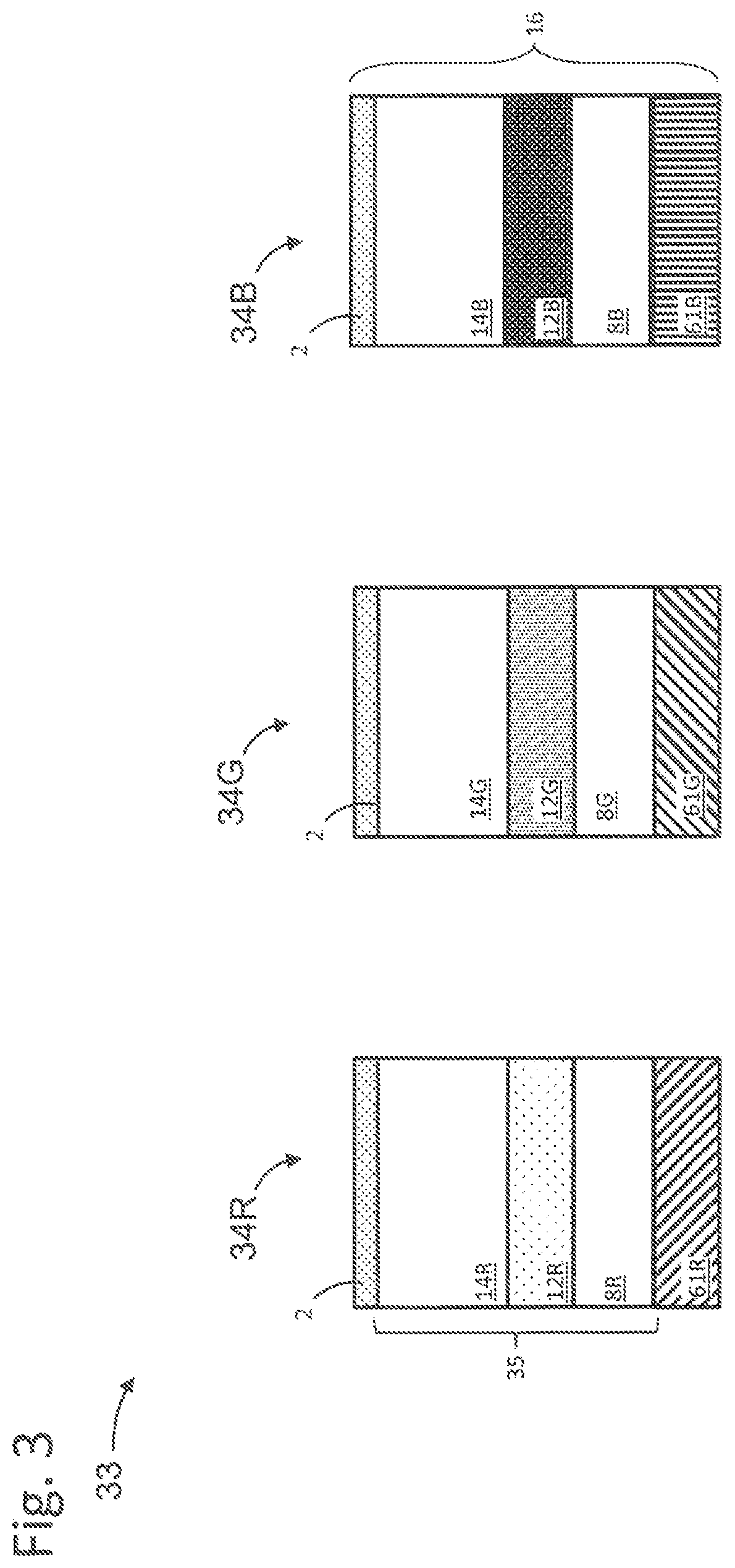
The patent describes an improved arrangement for an emissive display pixel using a reflective electrode and quantum dots or organic electroluminescent material. This arrangement includes multiple sub-pixels, each emitting light of different colors or wavelengths. The sub-pixels are placed between layers of emissive material and conducting electrodes to form an optical cavity. The reflective electrode causes a specific phase shift with the emissive material, and the conducting layer introduces a phase shift that depends on the color of the associated sub-pixel. The patent describes both top-emitting and inverted structures for the display. This arrangement improves brightness and efficiency while reducing device and manufacturing complexity.

Problems solved by technology

Having different sub-pixel structures increases device complexity and leads to significant costs for fabrication, and often compromises are made in efficiency to achieve acceptable costs.
Other modifications described in the art that improve performance result in adding complexity to the fabrication of a cavity structure in an LED by adding additional processing steps such as roughening or patterning.
Further modifications described in the art add complexity by adding additional layers to the device.

Method used


Image

  • High-efficiency qled structures
  • High-efficiency qled structures
  • High-efficiency qled structures

Examples


Embodiment Construction

[0022]Embodiments of the present invention will now be described with reference to the drawings, wherein like reference numerals are used to refer to like elements throughout. It will be understood that the figures are not necessarily to scale.

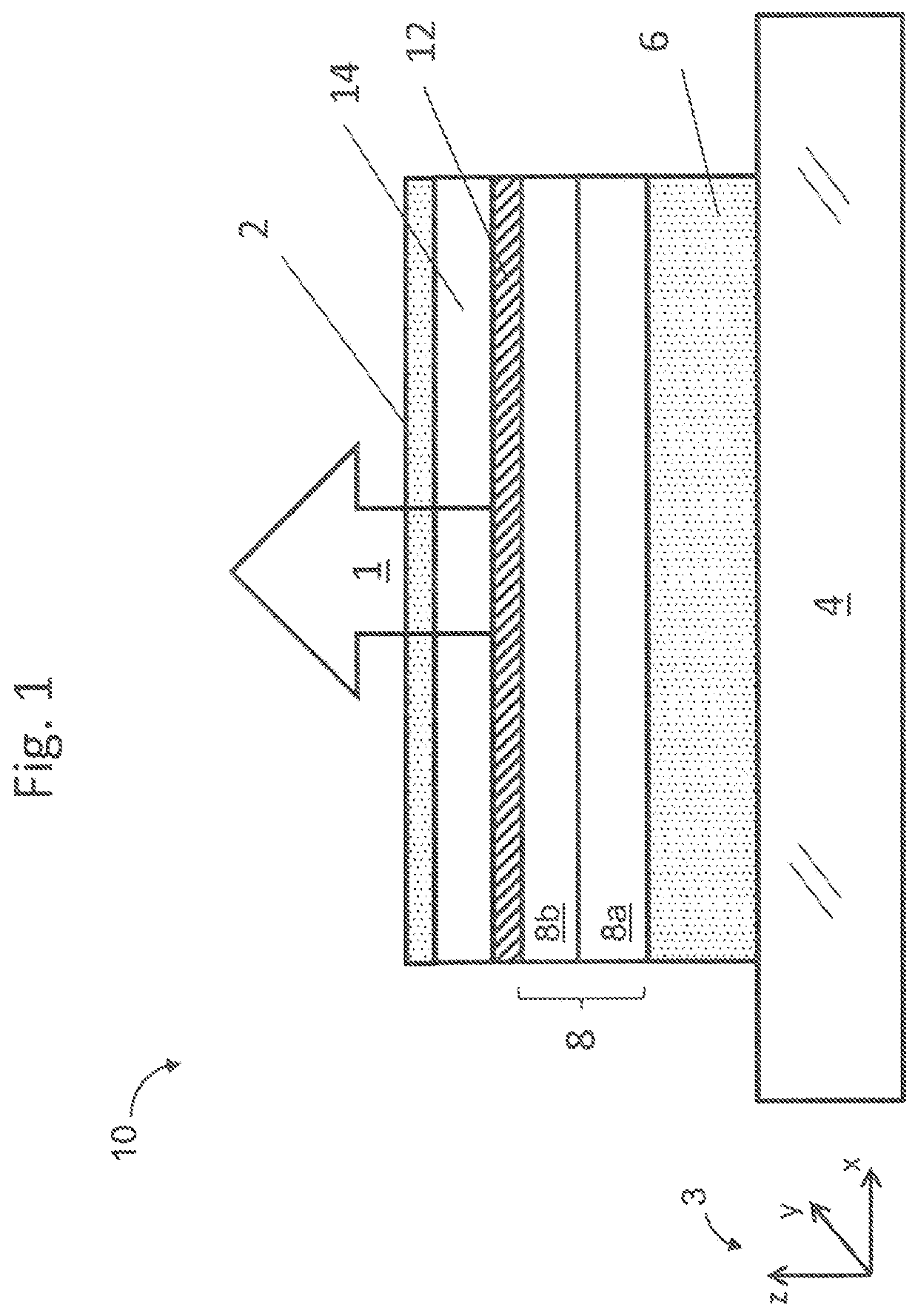
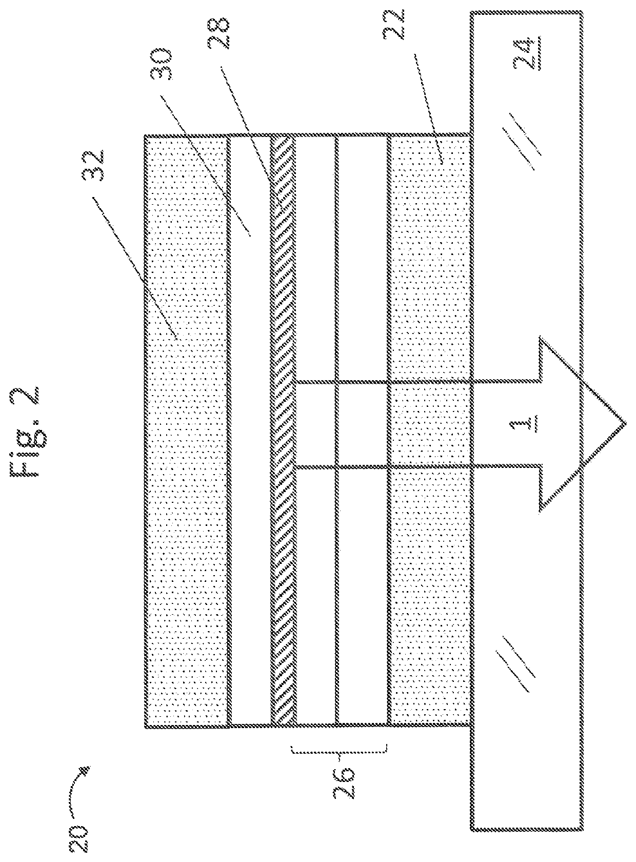
[0023]FIG. 1 is a drawing depicting an exemplary top emitting (TE) light-emitting device structure 10. The TE structure 10 emits light 1 through a top conducting layer, a top electrode 2, that is a partial reflector formed opposite from a substrate 4. The substrate 4 may be a glass substrate on which a bottom conducting layer, a bottom electrode 6, is formed. The thickness of the bottom electrode 6 may be greater than 80 nm. The bottom electrode 6 may be a metallic material configured to reflect light to enhance emission through the top electrode 2. The bottom electrode 6 is typically aluminum, silver, Indium Tin Oxide (ITO), and the like or a combination thereof. The bottom electrode 6 may be connected to a voltage source for applying differe...


PUM


Abstract

A light-emitting layer structure that maximizes constructive interference for light emission by varying a phase shift introduced by reflective electrodes. The light-emitting layer structure includes a first and second optical cavity including a first and second reflective electrode; a first and second partially transparent electrode; and a first and second emissive layer (EML) disposed between the first and second reflective electrodes and the first and second partially transparent electrodes, wherein the first EML emits light having a first wavelength; wherein the first reflective electrode introduces a first phase shift, depending on the first wavelength, on reflection of light emitted by the first EML; and wherein the second EML emits light having a second wavelength and the second reflective electrode introduces a second phase shift, depending on the second wavelength, on reflection of light emitted by the second EML, and the first phase shift is different from the second phase shift.

Description

RELATED APPLICATIONS[0001]This application is a continuation-in-part of U.S. application Ser. No. 16 / 517,971, filed on Jul. 22, 2019.TECHNICAL FIELD[0002]The present invention relates to a layer structure used in emissive devices, and, particularly, quantum dot (QD) light emitting diodes (QLEDs). QLEDs incorporating the present invention are used in displays to reduce complexity in the fabrication of the device while minimizing off-axis color shift and maximizing device efficiency.BACKGROUND ART[0003]Optical cavities are well known in semiconductor laser fabrication as described in U.S. Pat. No. 7,324,574 (Kim, issued Jan. 29, 2008). The use of cavities with organic LEDs (OLEDs) and QLEDs is also known as shown in US 2006 / 0158098 (Raychaudhuri et al., published Jul. 20, 2006), U.S. Pat. No. 9,583,727 (Cho et al., issued Feb. 28, 2017), and U.S. Pat. No. 8,471,268 (Moon et al., issued Jun. 25, 2013). Raychaudhuri et al. describe a top emitting OLED structure, and Cho et al. and Moon ...

Claims


Application Information

Patent Timeline
IPC IPC(8): H01L51/52H01L51/50
CPCH01L51/5265H01L2251/558H01L51/502H10K59/30H10K50/11H10K2101/40H10K50/13H10K50/115H10K50/156H10K50/818H10K50/828H10K50/852H10K50/856H10K2102/351H10K50/81H10K50/82
Inventor MONTGOMERY, DAVID JAMESBOARDMAN, EDWARD ANDREWSMEETON, TIM MICHAEL
Owner SHARP KK
Learn More