Superconducting nanowire single-photon detector, and a method for obtaining such detector

a single-photon detector and superconducting nanowire technology, applied in the direction of superconductor devices, optical radiation measurement, instruments, etc., can solve the problems of limited academic research application, inability to operate the detector inside a large cryogenic refrigerator, and high cost of packaging snspds, etc., to achieve long wavelength light, reduce heat capacity, and reduce the effect of cos

Pending Publication Date: 2021-03-18
FUNDACIO INST DE CIENCIES FOT NIQUES
View PDF0 Cites 0 Cited by
  • Summary
  • Abstract
  • Description
  • Claims
  • Application Information

AI Technical Summary

Benefits of technology

[0039]The types of 2D superconductors used in the present invention (i.e. high-Tc cuprate superconductors) can exhibit superconductivity in layers that are up to 10× thinner than for sputtered materials. This leads to a reduced heat capacity and therefore the detectivity of longer wavelength light. In addition the hot-spots can be larger, and the nanowire can be therefore wider, making fabrication much more reliable.
[0040]2D high-Tc cuprate superconductor materials are ultra-clean, single crystals, with a low intrinsic carrier density. Therefore they do not suffer inhomogeneities at grain boundaries, while heavily limit fabrication reliability in traditional SNSPDs. Therefore more precise and uniform patterning should be possible, leading to a lower dark count and potentially improved jitter time.
[0041]Also, the high-Tc cuprate superconductor materials used in the present invention as any 2D material, can be transferred and fabricated on any

Problems solved by technology

Based on local heating and hot spot creation in ultra-thin superconducting (SC) nanowires, however, these detectors can be only operated inside large cryogenic refrigerators at ultra-low operation temperatures<3K.
This makes the packaging of SNSPDs extremely impractical and expensive, and their application is limited to academic research.
However, those already known detectors, such as that disclosed in U.S. Pat. No. 6,812,464B1, have several drawbacks, mainly associat

Method used


Image

  • Superconducting nanowire single-photon detector, and a method for obtaining such detector
  • Superconducting nanowire single-photon detector, and a method for obtaining such detector
  • Superconducting nanowire single-photon detector, and a method for obtaining such detector

Examples


Embodiment Construction

lass="d_n">[0072]In the present section some working embodiments of the detector and method of the present invention will be described in detail.

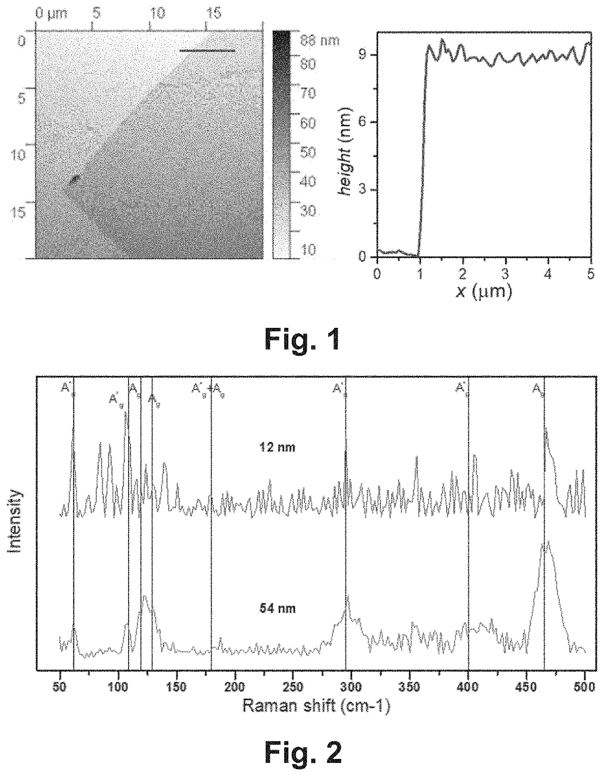
[0073]Particularly, a SNSPD with a very thin film thickness has been built by the present inventors in order to allow a reasonable detector performance, using the high-Tc cuprate superconductor Bismuth Strontium Calcium Copper Oxide (BSCCO). BSCCO belongs to the entirely novel class of strictly two-dimensional (2D) van der Waals (vdW) materials, which only recently have emerged. In contrast to other high-Tc superconductors BSCCO can be mechanically prepared with a film thickness of 1.5 nm corresponding to only half a crystallographic unit cell. In addition, being ‘cousins’ of the wonder material graphene, these ultra-clean single-crystals have far superior material quality than the strongly disordered superconductor thin films of NbN or WSi which are used for state-of-the-art SNSPDs. Having a >10 times reduced thickness, 2D superconductors ...


PUM


Abstract

The present invention relates to a superconducting nanowire single-photon detector, which can include a superconducting nanowire configured and arranged for the incidence of a photon on a region thereof and the formation, on that region, of a localized non-superconducting region or hotspot.
The superconducting nanowire is made of a high-Tc cuprate superconductor material having a superconducting critical temperature above 77 K.
The present invention also relates to a method for obtaining the superconducting nanowire single-photon detector of the present invention.

Description

CROSS-REFERENCE TO RELATED APPLICATIONS[0001]This application is based on and claims the benefit of priority from European Patent Application No. 19382806, filed on Sep. 17, 2019, the contents of which are expressly incorporated by reference herein.[0002]The project leading to this application has received funding from the European Union's Horizon 2020 research and innovation programme under grant agreement 820378.FIELD OF THE INVENTION[0003]The present invention relates, in a first aspect, to a superconducting nanowire single-photon detector which can operate above the temperature corresponding to the boiling point of liquid nitrogen.[0004]A second aspect of the present invention relates to a method for obtaining the superconducting nanowire single-photon detector of the first aspect of the present invention.BACKGROUND OF THE INVENTION[0005]In recent years Superconducting Nanowire Single-Photon Detectors (SNSPD), also known just as Superconducting Single-Photon Detectors (SSPDs), h...

Claims


Application Information

Patent Timeline
IPC IPC(8): H01L31/0352H01L31/09H01L31/18H01L39/10H01L39/16H01L39/24G01J1/42
CPCH01L31/0352H01L31/09H01L31/18H01L39/10H01L31/024H01L39/2422H01L39/2467G01J1/42H01L39/16H01L31/101G01J1/44G01J2001/442H10N60/84H10N60/857H10N60/0268H10N60/0801G01J1/0209G01J1/0252B82Y20/00H01L31/0203H10N60/30H10N60/0296H10N60/0688
Inventor EFETOV, DIMITRI K.LU, XIAOBOALI, AAMIR M.SEIFERT, PAULDURÁN, JOSÉ
Owner FUNDACIO INST DE CIENCIES FOT NIQUES
Why Eureka
Try Eureka