Infrared detecting element, method of manufacturing the same and temperature measuring device

Inactive Publication Date: 2005-06-21
SEIKO EPSON CORP
View PDF13 Cites 19 Cited by
  • Summary
  • Abstract
  • Description
  • Claims
  • Application Information

AI Technical Summary

Benefits of technology

[0029]As the semiconductor substrate, a P-conduction type silicon substrate may be used, but an N-conduction type is preferred. When a diode is formed on the P-conduction type silicon substrate, an N inversion layer is formed below an insulating layer provided on the surface of the silicon substrate, and a reverse current flows through the N inversion layer to deteriorate the forward characteristics of the diode. On the other hand, with the N-type silicon substrate, the N inversion layer is not formed to obtain the good forward characteristics of the diode, thereby permitting accurate temperature measurement.
[0030]In this way, by using the infrared detecting element of the present invention, the temperature measuring device capable of temperature measurement with high precision can b

Problems solved by technology

Therefore, it cannot be said that the accurate temperature of the cold junctions is detected.
Thus, a large error possibly occurs in the body temperature determined as describ

Method used


Image

  • Infrared detecting element, method of manufacturing the same and temperature measuring device
  • Infrared detecting element, method of manufacturing the same and temperature measuring device
  • Infrared detecting element, method of manufacturing the same and temperature measuring device

Examples


Embodiment Construction

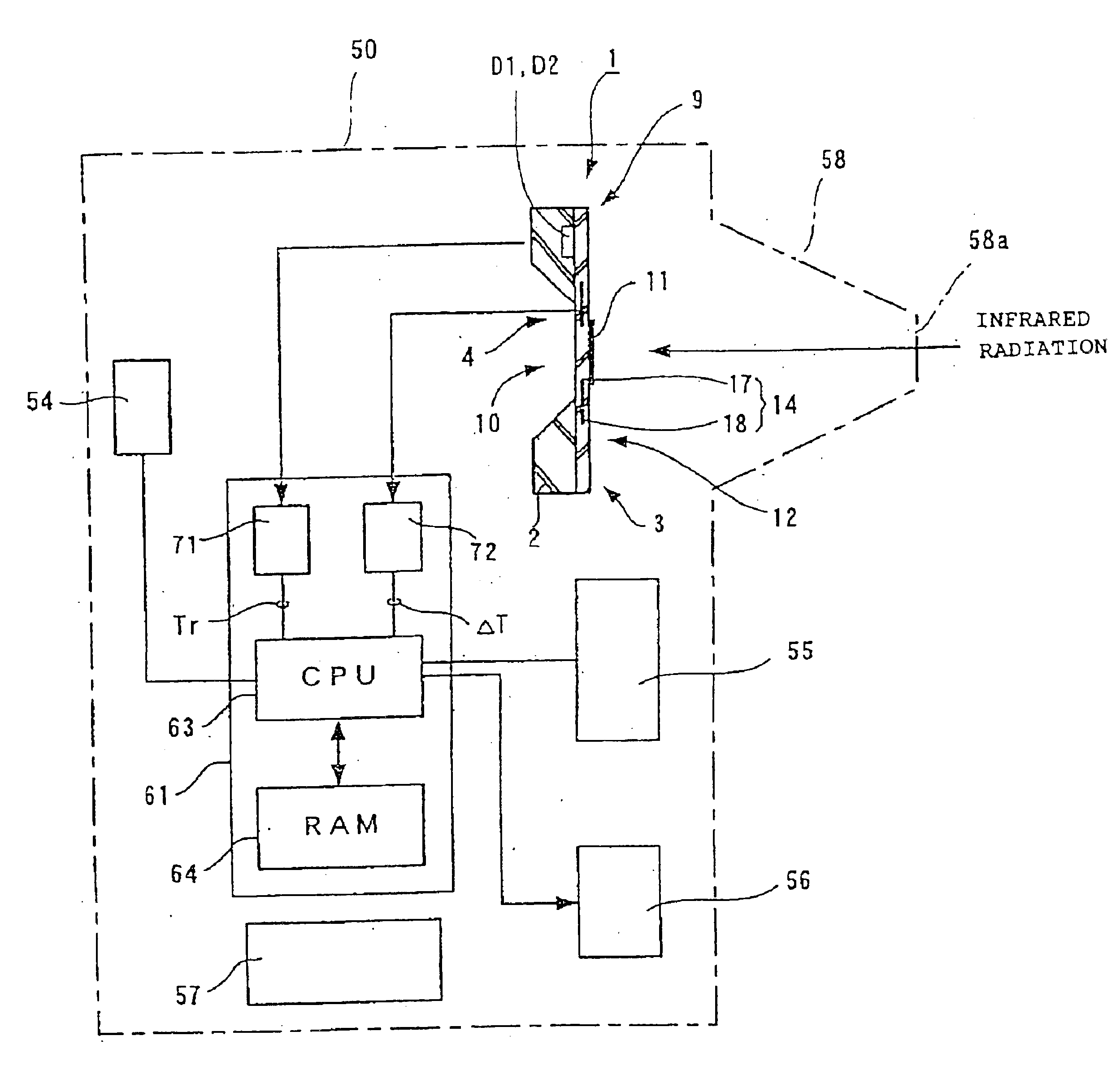
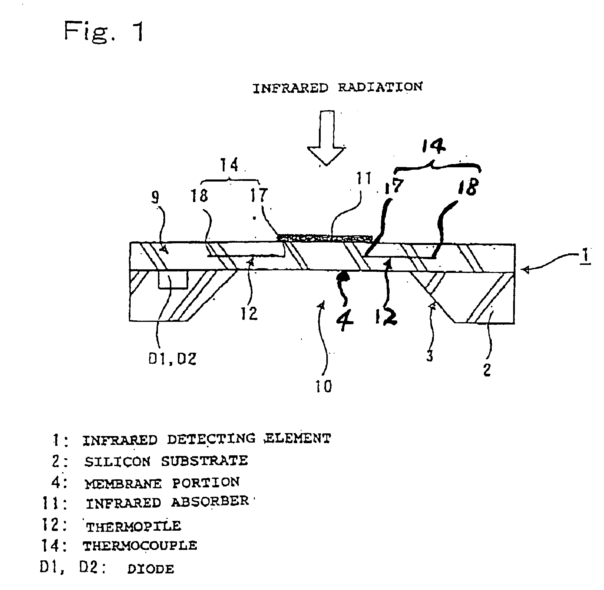
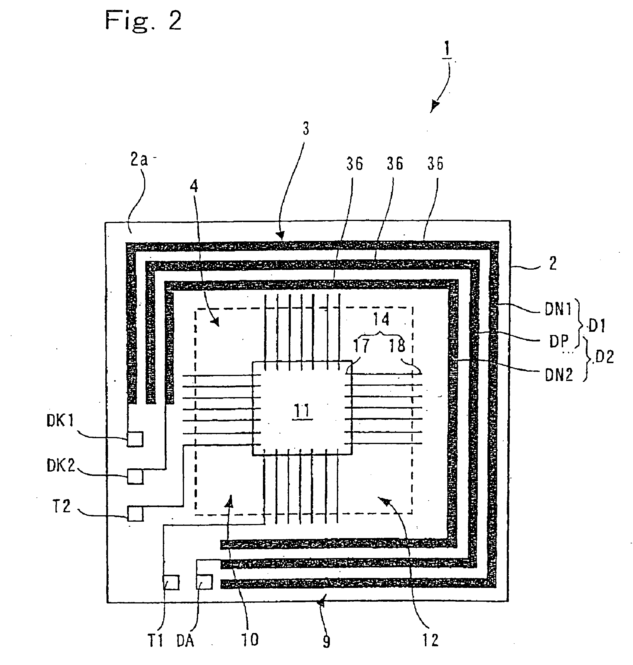
[0058]The present invention is described in further detail below with reference to the drawings. FIG. 1 shows the schematic construction of an infrared detecting element.

[0059]An infrared detecting element 1 of an embodiment comprises a silicon substrate 2 having a structure in which a central portion 10 is removed by etching from below to leave a membrane as a membrane portion 4 in the central portion 10, and an unetched portion as a thick wall portion 3 after etching of the silicon substrate 2. Also, gold black is deposited in a substantially square shape on the upper surface of the membrane portion 4 by sputtering vapor deposition or the like to form an infrared absorber 11.

[0060]The infrared detecting element 1 comprises a plurality of thermocouples 14 arranged on the four sides of the infrared absorber 11. The hot junction 17 of each of the thermocouples 14 is arranged below the infrared absorber 11 of the membrane portion 4, and the cold junction 18 of each of the thermocouple...


PUM


Abstract

To provide a thermopile infrared detecting element capable of accurate temperature measurement at low cost. An infrared detecting element 1 using a silicon nitride film as a first structure layer 22 constituting a structure of a membrane portion 4 is provided. Unlike silicon oxide, the first structure layer 22 has internal stress in the tensile direction, and can thus prevent the occurrence of bending. Also, diodes D1 and D2 can be formed in a silicon substrate 2 by using the first structure layer 22 as an element isolation region, and thus deformation of a thermopile 12 due to a change in the environment can be prevented to suppress measurement error of the thermopile 12. Furthermore, a high accuracy infrared detecting element capable of accurately detecting the temperature of cold junctions using the diodes D1 and D2 can be provided.

Description

BACKGROUND OF THE INVENTION[0001]1. Technical Field[0002]The present invention relates to a thermopile infrared detecting element and a method of manufacturing the same.[0003]2. Background Art[0004]Infrared radiation is emitted from the surface of a human body in an amount according to the body temperature, and ears have the normal temperature like the axillae. Therefore, clinical ear thermometers (temperature measuring devices) for measuring the body temperatures by detecting infrared radiation emitted in the ear cavities are known. In the clinical ear thermometers, the body temperatures are determined based on output from infrared detecting elements for converting received infrared radiation into electrical signals. Although various types of elements such as a pyroelectric type, a thermopile type, and the like are generally known as infrared detecting elements, thermopile-type infrared detecting elements having the merit of permitting mass production using a semiconductor manufact...

Claims


Application Information

Patent Timeline
IPC IPC(8): G01J5/12G01J5/16H01L23/00A61B5/01
CPCG01J5/16
Inventor SATO, SHIGEMIYAMASHITA, HIDETOHAGIHARA, TSUTOMU
Owner SEIKO EPSON CORP
Why Eureka
Try Eureka