Eureka AIR delivers breakthrough ideas for toughest innovation challenges, trusted by R&D personnel around the world.

Electronic package and method for manufacturing the same

Active Publication Date: 2021-03-18
SILICONWARE PRECISION IND CO LTD
View PDF0 Cites 2 Cited by
  • Summary
  • Abstract
  • Description
  • Claims
  • Application Information

AI Technical Summary

Benefits of technology

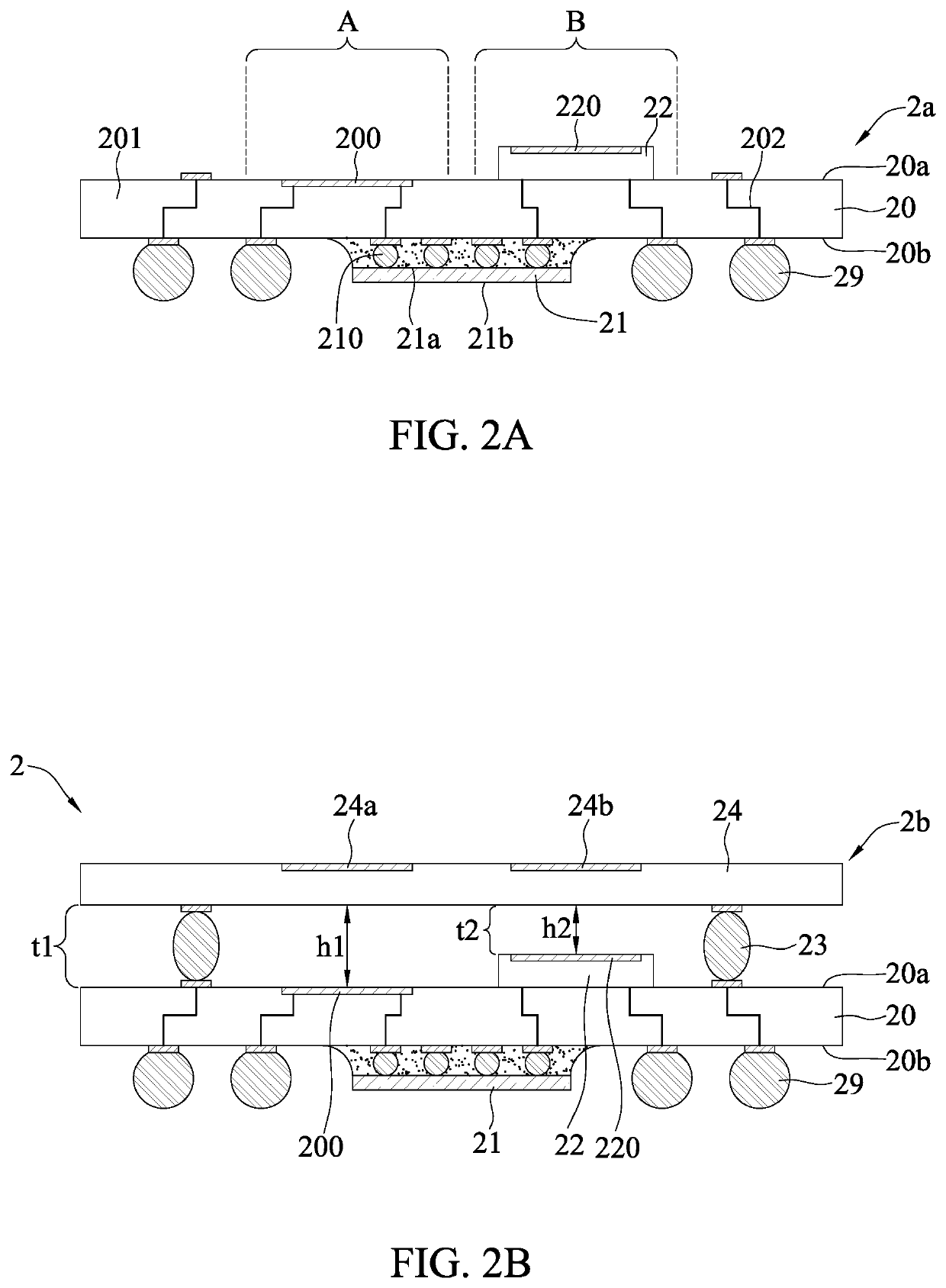
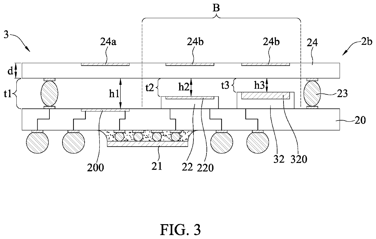
The present disclosure provides an electronic package and method of manufacturing the same that allows for the production of 5G millimeter wave (mmWave) at different frequencies using a substrate structure with a second antenna portion on a carrier structure with a first antenna portion. This antenna structure can produce different signals depending on the needs of the electronic component, improving the functionality of the antenna. Compared to prior art, the electronic package of the present disclosure increases the efficiency of the antenna, providing the necessary electrical functions for the 5G system. Additionally, the substrate structure is placed on the carrier structure, eliminating the need for extra layout areas and allowing for the production of antennas of various frequencies while maintaining small carrier structures size.

Problems solved by technology

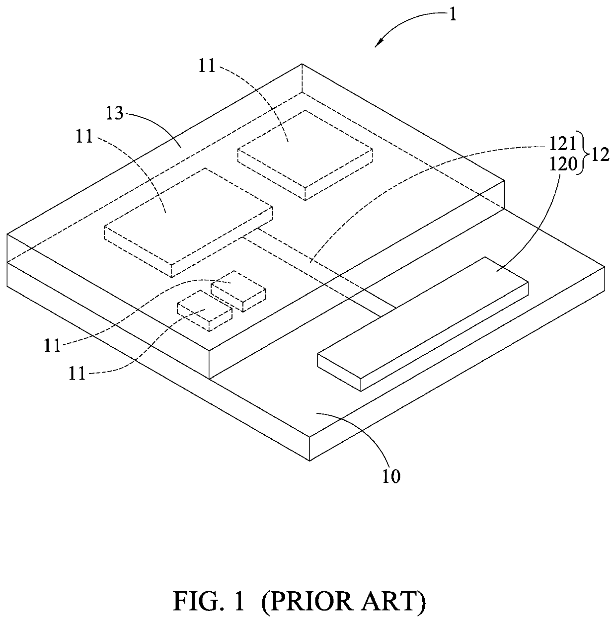
However, in the conventional wireless communication module 1, the antenna structure 12 is planar, and the dimensions of the substrate 10 are fixed, so there is only a limited space (layers) available for routing.
As a result, the wireless communication module 1 cannot provide the electrical functions required for running a 5G system, and it is difficult to meet the needs of 5G antenna operation.
Moreover, if more layout areas are added onto the surface of the substrate 10 in order to form antenna bodies 120 for a plurality of frequencies, it will inevitably increase the width of the substrate 10 and making it difficult to reduce the width of the wireless communication module 1.
As a result, the wireless communication module 1 cannot meet the requirements for miniaturization.

Method used


Image

  • Electronic package and method for manufacturing the same
  • Electronic package and method for manufacturing the same
  • Electronic package and method for manufacturing the same

Examples


Embodiment Construction

[0021]The implementations of present disclosure are illustrated using the following embodiments. One of ordinary skill in the art can readily appreciate other advantages and technical effects of the present disclosure upon reading the disclosure of this specification.

[0022]It should be noted that the structures, ratios, sizes shown in the drawings appended to this specification are to be construed in conjunction with the disclosure of this specification in order to facilitate understanding of those skilled in the art. They are not meant, in any ways, to limit the implementations of the present disclosure, and therefore have no substantial technical meaning. Without affecting the effects created and the objectives achieved by the present disclosure, any modifications, changes or adjustments to the structures, ratio relationships or sizes, are to be construed as falling within the scope covered by the technical contents disclosed herein. Meanwhile, terms such as “above,”“first,”“secon...


PUM


Abstract

An electronic package and a method for manufacturing the same are provided, where at least one substrate structure having a second antenna portion is disposed on a carrier structure having a first antenna portion, and then an antenna structure having a first antenna body and a second antenna body is stacked on the carrier structure by a plurality of supporting members to cover the first antenna portion and the second antenna portion, so that the first antenna body corresponds to the first antenna portion, and the second antenna body corresponds to the second antenna portion. The substrate structure is disposed on the carrier structure to generate 5G millimeter waves of different frequencies, such that the antenna structure can generate different antenna signals based on needs.

Description

BACKGROUND1. Technical Field[0001]The present disclosure relates to an electronic package, and more particularly, to an electronic package with an antenna structure and a method for manufacturing the same.2. Description of Related Art[0002]Wireless communication technology has now been widely applied to a myriad of consumer electronic products (e.g., mobile phones, tablets, and the like) for receiving and transmitting various kinds of wireless signals. To satisfy the demands for portability and ease of Internet access (for example, watching multimedia content) for consumers electronic products, wireless communication modules are designed and manufactured with lightweight and compact sizes in mind. Among them, patch antennae have been widely adopted in the wireless communication modules of electronic products due to their characteristics such as small volume, light weight and ease to manufacture.[0003]With the improvements in image quality, multimedia content nowadays tends to have v...

Claims


Application Information

Patent Timeline
IPC IPC(8): H01Q9/04H01Q1/38
CPCH01Q9/0414H01Q1/38H01L23/58H01L23/3128H01L23/49816H01L25/16H01L21/561H01Q1/2283
Inventor TUNG, CHENG-PIAOTSAI, WEN-JUNG
Owner SILICONWARE PRECISION IND CO LTD
Why Eureka
Eureka Blog
Learn More