Semiconductor Device and Power Conversion Device
a technology of a power conversion device and a semiconductor, which is applied in the direction of semiconductor devices, basic electric elements, electrical appliances, etc., can solve the problems of global warming becoming an important worldwide urgent problem, and achieve the effects of improving a trade-off relationship, low conduction loss, and low switching loss
- Summary
- Abstract
- Description
- Claims
- Application Information
AI Technical Summary
Benefits of technology
Problems solved by technology
Method used
Image

Examples
first embodiment
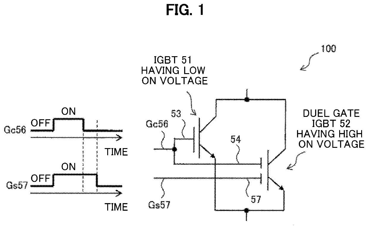
[0058]FIG. 1 is a diagram showing an example of a circuit configuration of a semiconductor device 100 according to the embodiment first embodiment. As shown in FIG. 1, the semiconductor device 100 is implemented by connecting in parallel an IGBT 51 and an IGBT 52 that have different performances from each other. The IGBT 51 has a small voltage drop when a predetermined current flows, that is, a low ON voltage performance. In contrast, the IGBT 52 is a dual gate IGBT that has a high ON voltage performance and includes two independent and controllable gates.
[0059]A gate 53 of the IGBT 51 having a low ON voltage and a gate 54 of the dual gate IGBT 52 having a high ON voltage are electrically connected with each other. A same gate control signal Gc 56 is supplied to the gates 53 and 54 that are connected with each other. Hereinafter, the gates 53 and 54 are collectively referred to as a Gc gate 56. In contrast, a gate control signal Gs 57 is applied to the gate 57 of the dual gate IGBT ...
second embodiment
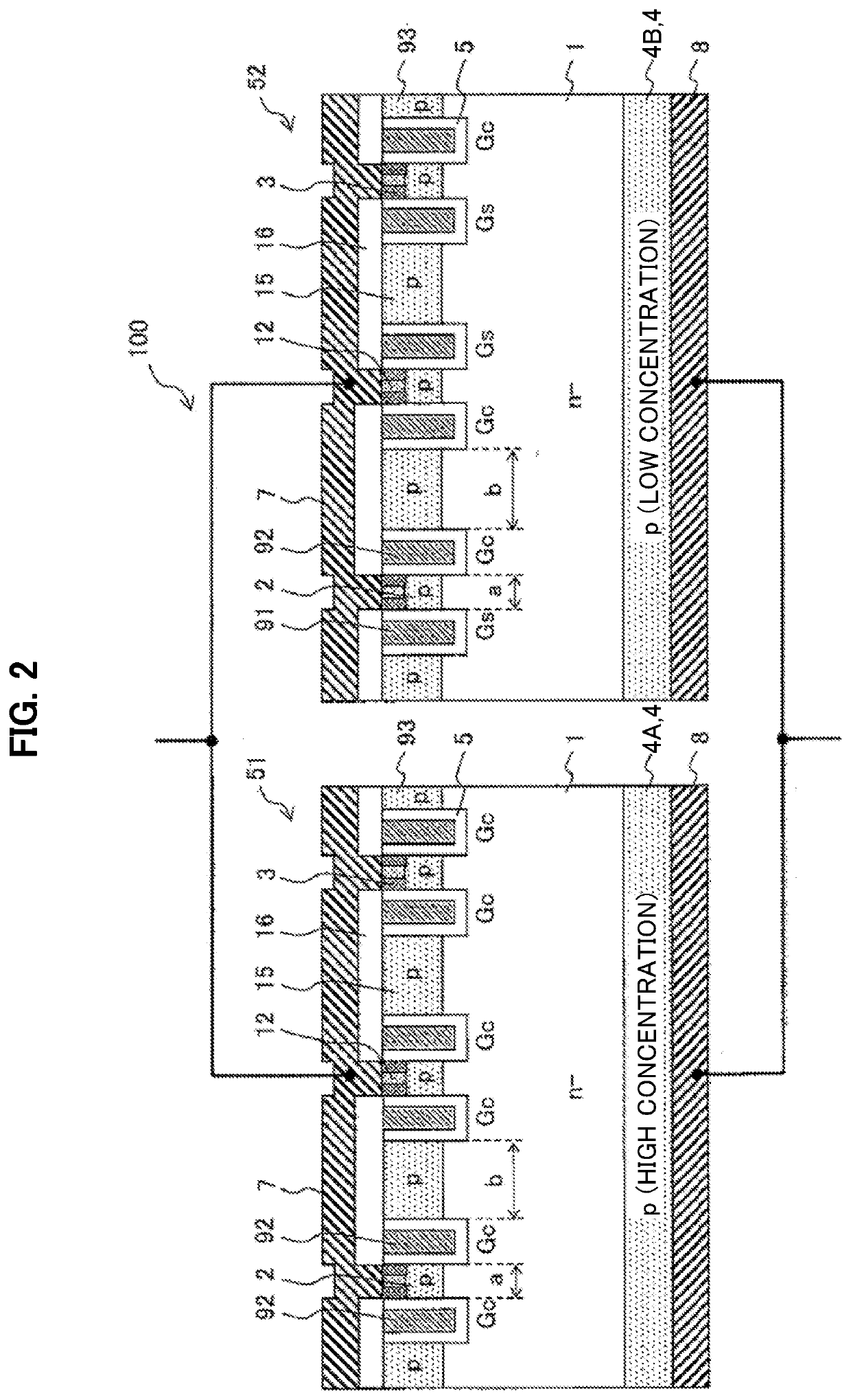
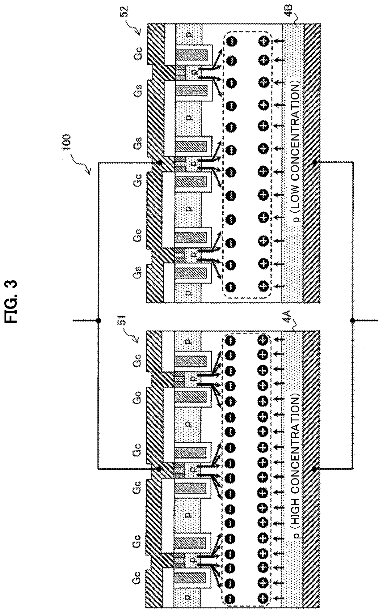
[0101]FIG. 9 is a diagram showing an example of a cross-sectional structure of a semiconductor device including IGBTs 51a and 52a that form a semiconductor device 200 according to the second embodiment of the invention. A circuit configuration of the semiconductor device 200 according to the second embodiment is the same as a circuit configuration of the semiconductor device 100 according to the first embodiment as shown in FIG. 1. A cross-sectional structure of the IGBT 51a and the IGBT 52a that form the semiconductor device 200 according to the second embodiment is substantially the same as a cross-sectional structure of the IGBT 51 and the IGBT 52 according to the first embodiment as shown in FIG. 2. Hereinafter, differences of the second embodiment from the first embodiment will be mainly described.
[0102]As shown in FIG. 9, the IGBT 51a includes a plurality of trench-shaped Gc gates 92 as gate electrodes. The same gate control signal Gc 56 is applied to all of the Gc gates 92. I...
third embodiment
[0121]FIG. 12 is a diagram showing an example of a cross-sectional structure of a semiconductor device including two IGBTs 51b and 52b that form a semiconductor device 300 according to the third embodiment of the invention. A circuit configuration of the semiconductor device 300 according to the third embodiment is the same as a circuit configuration of the semiconductor device 100 according to the first embodiment as shown in FIG. 1. A cross-sectional structure of the IGBT 51b and the IGBT 52b that form the semiconductor device 300 according to the third embodiment is substantially the same as a cross-sectional structure of the IGBT 51 and the IGBT 52 according to the first embodiment as shown in FIG. 2. Hereinafter, differences of the third embodiment from the first embodiment will be mainly described.
[0122]In the first embodiment (see FIG. 2), the gate electrodes (the Gs gates 91 and the Gc gates 92) are embedded in trenches formed in a base body portion of a semiconductor. In co...
PUM
| Property | Measurement | Unit |
|---|---|---|
| conductive | aaaaa | aaaaa |
| voltage | aaaaa | aaaaa |
| conducting | aaaaa | aaaaa |
Abstract
Description
Claims
Application Information