
Solid-state imaging device, method for driving solid-state imaging device, and electronic apparatus

a solid-state imaging and imaging device technology, applied in the direction of radio frequency controlled devices, instruments, television systems, etc., can solve the problems of puf response inevitably containing noise and error induced by noise, and the immediate signal output of the sensor chip is not always protected, so as to prevent forgery and falsification of images, and prevent an increase in data to be saved

Active Publication Date: 2021-04-29
BRILLNICS JAPAN +1
View PDF5 Cites 2 Cited by
  • Summary
  • Abstract
  • Description
  • Claims
  • Application Information

AI Technical Summary

Benefits of technology

The invention aims to improve image security by eliminating the need for multiple response measurements and preventing data to be saved in a fuzzy extractor when an initial key is generated. The result is a unique and highly confidential response data that can prevent forgery and falsification of images.

Problems solved by technology

If the acquired data is falsified, serious results such as accidents may be caused.
The conventional encryption technique protects digital signals output from the microcomputer chips but does not always protect immediate signals output from the sensor chips.
The PUF response inevitably contains errors induced by noise.
Thus, when generating an initial key, the fuzzy extractor is disadvantageously required to save increased amount of data.
In this way, the identification data cannot be correctly generated when the information relating to the unique key is absent.
On a substrate surface for forming the photodiodes (PDs), there is a surface level due to dangling bonds or other defects, and therefore, a lot of charges (dark current) are generated due to heat energy, so that signals fail to be read out correctly.
The variations is affected by random noise, which accumulates as each attempt is made.

Method used


Image

  • Solid-state imaging device, method for driving solid-state imaging device, and electronic apparatus
  • Solid-state imaging device, method for driving solid-state imaging device, and electronic apparatus
  • Solid-state imaging device, method for driving solid-state imaging device, and electronic apparatus

Examples


Embodiment Construction

[0052]Embodiments of the present invention will be hereinafter described with reference to the drawings.

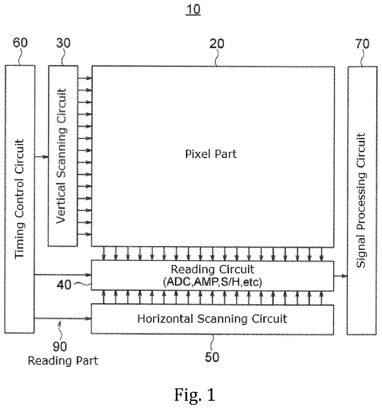
[0053]FIG. 1 is a block diagram showing an example configuration of a solid-state imaging device relating to an embodiment of the present invention. In this embodiment, a solid-state imaging device 10 is constituted by, for example, a CMOS image sensor.

[0054]As shown in FIG. 1, the solid-state imaging device 10 is constituted mainly by a pixel part 20 serving as an image capturing part, a vertical scanning circuit (a row scanning circuit) 30, a reading circuit (a column reading circuit) 40, a horizontal scanning circuit (a column scanning circuit) 50, a timing control circuit 60, and a signal processing circuit 70. Among these components, for example, the vertical scanning circuit 30, the reading circuit 40, the horizontal scanning circuit 50, and the timing control circuit 60 constitute the reading part 90 for reading out pixel signals.

[0055]The solid-state imaging device 10 rela...


PUM


Abstract

A solid-state imaging device includes a pixel part, a reading part for reading a pixel signal from the pixel part and a response data generating part including a fuzzy extractor. The response data generating part generates response data including a unique key in association with at least one selected from among variation information of pixels and variation information of the reading part. The response data generating part generates, when regenerating a key, a unique key using helper data acquired in generation of an initial key, variation information acquired in the regeneration of the key, and reliability information determined based on the variation information acquired in the regeneration of the key.

Description

TECHNICAL FIELD[0001]The present invention relates to a solid-state imaging device, a method for driving a solid-state imaging device, and an electronic apparatus.BACKGROUND[0002]Solid-state imaging devices (image sensors) including photoelectric conversion elements for detecting light and generating charges are embodied as CMOS (complementary metal oxide semiconductor) image sensors, which have been in practical use. The CMOS image sensors have been widely applied as parts of various types of electronic apparatuses such as digital cameras, video cameras, surveillance cameras, medical endoscopes, personal computers (PCs), mobile phones and other portable terminals (mobile devices).[0003]As mentioned above, the CMOS image sensors are used to optically capture images in a wide range of application fields and thus have a large market. The demand for the CMOS image sensors is expected to keep growing in the future due to the increase in the CMOS image sensor applications including vehic...

Claims


Application Information

Patent Timeline
IPC IPC(8): H04N5/378H04N5/347H01L27/146H04N5/367H04N5/374
CPCH04N5/378H04N5/347H01L27/14643H04N5/367H04N5/374H01L27/14609H04N1/028G09C5/00H04L9/10H04N25/00H04N25/76H04N25/78H04N25/75H04N25/46H04N25/68
Inventor OKURA, SHUNSUKESHIRAHATA, MASAYOSHIFUJINO, TAKESHISHIOZAKI, MITSURUKUBOTA, TAKAYA
Owner BRILLNICS JAPAN
Learn More