

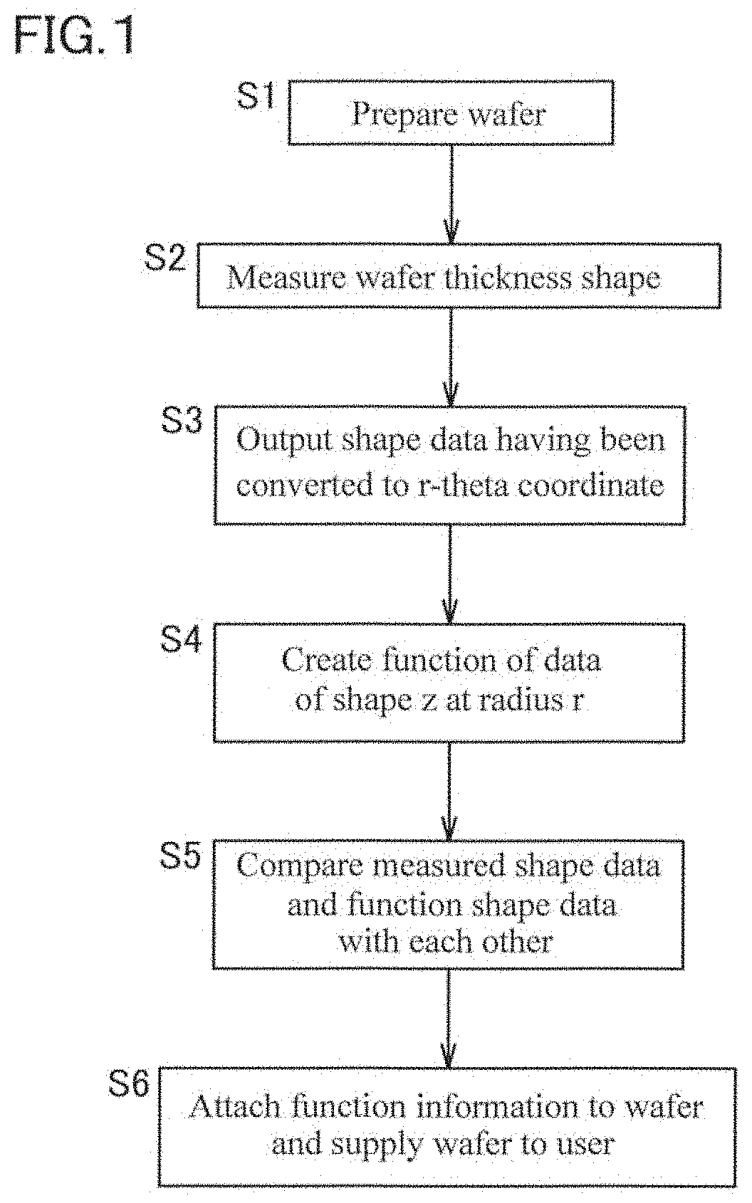
Method for creating wafer shape data
a technology of shape data and data, applied in the direction of measurement devices, semiconductor/solid-state device testing/measurement, instruments, etc., can solve the problems of inability to obtain the shape of the entire surface of the wafer, error with respect to the actual cross-sectional shape, and inability to achieve high accuracy the effect of wafer shape measuremen
- Summary
- Abstract
- Description
- Claims
- Application Information
AI Technical Summary
Benefits of technology
Problems solved by technology
Method used
Image

Examples
example 1
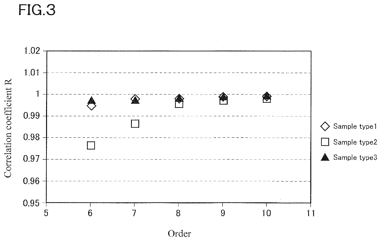
[0044]A relationship between an order of the polynomial and a correlation coefficient has been examined. Specifically, three silicon wafers (hereinafter, each referred to as wafer) each having a diameter of 300 mm were prepared, and the thickness shape of each wafer was measured by a flatness measuring machine “WaferSight2” manufactured by KLA-Tencor. The WaferSight2 is a measuring machine operating based on the principle in which light is incident on a wafer, and a shift amount on the surface of the wafer is measured according to the number and the widths of interference fringes generated by optical interference between light reflected by the wafer and light reflected by a basic plane.
[0045]A file (wnt file) of the measurement result outputted by the WaferSight2 was converted to a measured thickness value for the polar coordinate having an originating point at the center of the wafer, by using off-line analysis software “OASys” manufactured by KLA-Tencor, and the measured shape dat...
example 2
[0050]15 silicon wafers (hereinafter, each referred to as wafer) each having a diameter of 300 mm were prepared, and creation of the function was performed for each wafer according to the procedure shown in FIG. 1, and the thickness map from the obtained function and the thickness map outputted from a measuring machine were compared with each other. Specifically, the thickness shape of each wafer was measured by the flatness measuring machine “WaferSight2” manufactured by KLA-Tencor.
[0051]A file (wnt file) of the measurement result outputted by the WaferSight2 was converted to a measured thickness value for the polar coordinate having an originating point at the center of the wafer, by using off-line analysis software “OASys” manufactured by KLA-Tencor, and the measured shape data having been converted was outputted as a csv file. For the measured shape data having been outputted, the θ interval (split angle θ1) was one degree, and the interval in the r direction was 0.2 mm.
[0052]Ap...
PUM
 Abstract
Description
Claims
Application Information